 |
||
|
||
| ||
|
||
|
||
| ||
of AMD64 architectureForewordThe 8th generation of AMD processors - Opteron and Athlon 64 - has reached our region for some time already. Our readers might have been asking why we had been tarrying with a review. The answer is simple - we posed a more interesting (and ambitious) aim - to examine its microarchitecture in depth and detail, examine its behaviour, and compose the most complete description of the K8 generation architecture. But first let's perform an easier task - understand the nuances of microarchitecture operation. And you, the reader, will determine the level of our success. First, let's remember that a rather detailed review of K8 microarchitecture (as detailed as possible at that moment) has already hit our pages about six months ago. Since that time we haven't stumbled upon anything as thorough as that, so you might start with Facts & Assumptions about the Architecture of AMD Opteron and Athlon 64 in detail describing the Hammer architecture. But, as we remember, that review brought up a number of questions and assumptions that we'll try to make clear and comment if needed. Platforms testedLet's list the tools required for our examination. Opteron platform:
Pentium 4 platform:
This equipment list already enables us to:
Any test is, first of all, the method, so let's determine it. As a rule, testing a new platform requires clear understanding of all nuances. In order to do this, let's use synthetic tests to "penetrate" the K8 architecture. The plan is:
We admit the task is a non-trivial one. The thing is that the attitude to either product positioning might be very different. It can happen so that a product might look better or worse just on the background of its rival. To avoid this we'll try to use the maximum number of tests and choose conforming rivals. And at any cost we shouldn't forget our readers browsing this review to decide if it's worth messing with this architecture anyway. What killer apps does it have? Would K8 be a breakthrough as AMD promised? Would it be of use in games? In videoconferencing? As a server or workstation platform?! What about the prospects? All these are questions we have to give answers to, so this article can hardly be overestimated. Now let me introduce the team. The thing is that, having aimed at maximum objectivity, we decided to try absolutely new reviewing method - teamwork. This article has not one, two, or even three authors; it's a completely collective product. So, the list of authors is below:
Besides, these guys provided us with invaluable help both in criticism, and goal setting:
You can see the team is pretty big. But we shouldn't forget about another part compulsory for any review, i.e. practice. This where the iXBT team enters:
All participants are not newbies by any means, we believe this should tell upon the review well. There's only one little role left for me, Victor Kartunov aka matik. It turned so that I am the author of most of the previous Hammer reviews for iXBT. This one is not an exception as well. Let's see if AMD fulfils what I've "promised" before.
Well, I guess it's high time now to start the review at last, before this foreword bores you. :-) Opteron seriesLet's revise processors that AMD announced on April 22 (a natural field-day! :-). Like forecasted in the previous article, AMD started storming the server market. On April 22 Opteron processors were officially announced. It's interesting that since that time AMD hasn't been specifying any clock speeds or ratings. Instead the whole Opteron family is divided into three series - 1xx, 2xx and 8xx (or 100, 200, and 800, respectively). The difference is only that Opteron 1xx is for single-way systems, Opteron 2xx - for dual-way, and Opteron 8xx - for 8-way. In every series processors are distinguished by numbering. Initially, only the 2xx series was announced, with others (14x and 84x) released late in June. Initially the 2xx series included Opteron 240 (1400MHz), 242 (1600MHz) and 244 (1800MHz). On August 4 Opteron 246 (2GHz) was announced. Similar 146 and 846 are to arrive as well. Each processor has 128-bit (+16 bit ÅÑÑ) memory interface, triple Hyper Transport interface and 1024Kb L2 cache. This is the maximum cache we have expected in the previous article, and, as far as we know, the limiting for this core. Currently the processor supports Registered DDR266 and DDR333 with or without ECC. It seems after JEDEC approves ECC DDR400 we'll "stumble" upon similar support in Opteron. The reason to think so is the results of running Athlon 64 with DDR400, which it shouldn't support officially. It's interesting that Opteron is even capable of working with a single module. This surprised us, as remembering the memory bus was 128-bit we feared it wouldn't do. Of course, a single module halves memory bandwidth and, perhaps, changes the latency as well, as the payback. But the opportunity to run a system if one of two modules failed might be helpful. We've also expected the processor wouldn't work with unbuffered memory. As it has been said before, Opteron is designed for servers and workstations where Registered ECC is almost 100% compulsory. It's also interesting that you can install memory for only one processor. In this case the second will use it as well! :-) Well, I doubt anyone would be doing this, but such architecture flexibility excites respect. The dual-way platform runs with a single processor as well. Nothing surprising, but worth checking anyway. Cache subsystem. Analyzing changesCache subsystem performance is one of the important components of processor performance. Cache memory is called to negate the performance difference between RAM and processor, so it works on the front of all bottlenecks. As you know, K7 cache had some of them, so it would be very interesting to get to know what, except for the capacity, has changed in K8 comparing to Athlon XP. In general, cache performance depends on latency, throughput, as well as some other factors like associativity type (which we'll discuss later). The first two affect the performance significantly stronger than other. At that, latencies for random and sequential access might differ (and do differ, as you'll see below). So, we'll first describe the situation with Athlon XP cache design, and then compare it with K8 (here authors believe it's sensible to use this abbreviation, as Opteron and Athlon 64 have the same cache organization.) Let's look at the table of latencies for L1 and L2 caches of Athlon XP and K8:
We can see two variants for L2. What does "best" and "worse" mean? To explain this, let's remember such feature of AMD cache organization, as, "exclusive". Its idea is not to copy, but append L1 content to L2. This enables AMD to speak of total cache capacity as of L1 + L2.
However this cache organization has some features you should know of. First of all, Athlon XP has 64-bit bus between L1 and L2. Remember this, you'll need it later. Now let's look at these features on the example of Athlon XP cache. Feature #1: as requested or processed data are first of all stored in L1 cache, this might (and almost always does) overload L1. In this case, L1 must drop the oldest or useless data to L2 and then acquire new data (as it's not doubled in cache, we can't just delete the data). To handle data faster, the processor has a special Victim buffer for storing data to be dropped off to L2. This frees the space in L1 for newer data. This buffer is needed not because L1 and L2 delays differ, the Victim buffer relieves L1 cache from waiting for slower L2. Feature #2: For example, we requested data absent in L1, but present in L2. A natural situation, isn't it? In this case the delays will be:
In real life cache and Victim buffer almost always contain data. So, loaded, Athlon XP's L2 latency is drawn to the "worst". You should consider these features, if you are focused on the maximum performance. This might naturally bring up a question, "Why AMD has mixed up with exclusive cache organization at all? Here we should remind that Athlon XP now has 128Kb L1 cache and 256Kb L2 cache (later - 512Kb). So, it would be very senseless to lose half of the capacity for some trivial dubbing! I'm not even speaking that, according to AMD, the benefit of large L1 exceeds losses caused by more complex L1-L2 interaction. By the way, exactly such cache organization enabled to launch Duron with 64Kb L2 cache (twice as small as L1.) In case of usual inclusive architecture, this would be just senseless. So, considering that AMD still uses exclusive architecture, extending the L1-L2 bus seems to be a sensible way of improving the loaded operation. Intel did this in the Coppermine core, having implemented the ATC (Advanced Transfer Cache) with 256-bit L1-L2 bus. This explains our interest regarding the bus from the previous article. Besides, don't think "exclusive cache" is rubbish. This technology is a feature, not a disadvantage. In a manner, it's more about tests designed to load L1-L2 bus as much as possible. AMD is completely right saying this almost never occurs in real life. From the angle of theoretical bandwidth the fact that K7/K8 L2 loses to Pentium 4 cache is related to different ideology of these architectures. So, don't you be tricked by these "magic numbers" to make premature conclusions. And one more comment. In general, cache organizations do not differ only by being exclusive and inclusive. For example, L1 and L2 data might be updated by completely different algorithms, which make this interaction even more complex... But let's get back to L1-L2 bus width. Before we take a look at results of synthetic tests that answered this question we have to understand another cache feature - associativity. As you know, in general cache can map memory in different ways. These include partially and fully associative, direct-mapped cache. All of these differ by memory mapping. By the way, using different organizations, caches are updated by different algorithms. Still, this isn't related to the degree of associativity. Today the most popular is partial n-way associative cache. Actually n-way associative cache can map given memory string in any of its n ways. This is a sensible compromise between the fully associative and direct-mapped cache. The format can map any memory space in any cache space, but has extremely complex circuitry. Actually, as far as we know, it was used only once (!) - in Cyrix Cx686 CPU as L1 code cache sized just 256 bytes (8 strings!). The latter is much simpler as well as less effective, as data from different memory spaces might collide in the only cache string dedicated for them. K7 and K8 architectures feature 16-way partially associative L2. Now let's see how we can measure the width of aforementioned bus anyway. For example, if you start reading from L2 into L1, this must send data out of L1 into L2, as L1 is finite. So, in an ideal case (let's not argue if it's possible now) L1-L2 bus will be loaded with both data we requested and data sent from L1 to L2. Considered the bandwidth is maximal, the highest read/write speed we might achieve by this would be 64-bit/2, i.e. 4 bytes per clock. If we achieve anything higher, the bus should be wider than 64-bit. Still there's a nuance - if cache interaction doesn't fully meet the data exclusiveness requirement, we can get a situation when no data is pushed out. This requires additional examination to be carried out whenever possible. But anyway the indicative factor would be sequential read speed of an array larger than L2, but slower than L2+L1Data (1024 to 1088 Kb for K8). If cache works non-exclusively, some data will be pushed out into RAM resulting in speed decrease. However, if the high read speed keeps up, this will mean cache exclusiveness and double amount of data transferred (both from L2 to L1, and from L1 to L2). Exactly here exceeding the weight-average over 4 bytes/clock (i.e. over 8 bytes/clock in both ways) will stand for a bus wider than 64-bit! On the other hand, if K8 has bus wider than 64-bit, it should read a single cache string (64 bytes) in fewer clocks. Of course, it's sensible to make bus wide enough to read a string in an integer number of clocks - 128-bit or 256-bit. (It should be clear that wider buses are unreal and actually ineffective). There might be a composite variant as well, when we have two 64-bit buses (or some exotics with 128-bit on way and 64-bit another). Actually, there's not much sense in an asymmetrical bus, so we can figure the following:
So, we should try and invent a method to distinguish these somehow. To check for the 128-bit bus, let's read a 64-byte cache string cyclically starting from different positions. Alongside we'll be counting the amount of clocks required to load each 4-byte words (it's not that easy, as there's a lot of factors to consider.) If it reads 16 bytes per clock (128-bit bus), it should take 4 clocks total. Besides, having started from, say, the 3rd word, we would have get the string beginning at once or almost at once. However, it comes in the end of the cycle, by 8th clock like it's a normal 64-bus! Spoken simpler, caches exchange words that fit their interconnect bus best. By reading the string randomly we get different times. By offsetting the initial position and comparing the total string read time we can get the bus word size. This method showed us 64-bit words were read, i.e. the bus was 64-bit wide. Nevertheless, the test in 1024-1088 Kb space indicated that resulting performance exceeds 8 byte/clock that, together with absence of 128-bit bus proved in the previous paragraph, points to variant #3 only. Thus we can state that AMD advanced the L1-L2 cache bus in K8, so it now features two opposite 64-bit buses (64 + 64) instead of a single duplex 64-bit bus. This considerably reduces bottlenecks. By the way, this told upon the low-level tests at once - L2 cache speed had boosted by at least a quarter at the same clocks. It's also important that L1-L2 bottlenecks almost vanished and their possibility was reduced to minimum. The "worst" latency was reduced significantly as well. Those who want more details about the test method should read the Appendix 1 that contains a thorough description of L2 cache test methods and results. Decoders and pipelines. Internal units ideologyAs we've written in the previous article, one of the units that have been considerably changed in K8 was the x86 instruction decoder. Before we take a look at the particular changes, let's speak about architecture "ideology" or rather "concept" first. The thing is (and it's not a secret anymore) that internal instruction system of all x86 processors significantly differs from the external. So, if everything is clear about the latter, the former is not that understood. I.e. almost everybody into it knows that instructions are divided into simpler ones inside x86 (by the way, speaking of x86 instructions we mean AMD64 instructions as well; just not to mention this further). But it turns out that modern processors are so different from this point that we decided to put the existing information in a good order. But first let's familiarize the reader with the problem that made it necessary to transform the external instruction system into the internal. It's up to you to decide whether it's compulsory or not.
In general, any microprocessor architecture is aimed at maximum performance (we are not speaking of special chips like AMD Alchemy 1500 - the PDA market is less sensitive to such feature, as performance.) Striving for maximum demands compromises. So you should understand that some "disadvantages" are not the result of developers' dumbness, but a forced compromise to implement things that are more important. As for x86 processors, Intel and AMD chose different ways of achieving maximum performance. If you remember, simply speaking performance is clock speed multiplied by average instruction per clock. So, to increase performance we should increase either of them, or both. This is where the companies have chosen the different ways - Intel focused on clock speeds, AMD - on instructions per clock. Respectively, all further architecture differences are derived directly from the chosen concept. x86 instruction decoders of Pentium 4, K7 and K8 are not an exclusion. Besides, decoder design was affected by the fact that x86 instructions are way inconvenient for developers, because:
Because of all this, it turned out to be easier to "transform" x86 instructions into a number of regular internal instructions of fixed architecture to be sent to microprocessor's functional units (FU). Besides, such an internal instruction might include additional fields (e.g. simplifying operand searches.) To drawing a relative analogy, imagine a pipeline with mixed up materials and manuals that should be come a car in the end. Like it? Aha! Manufacturers do not like it as well. As a result they are forced to make efforts to put some order on the pipeline. And only having done this, they can continue construction. So I guess you understand now why order is required for high performance. Let's now remember that since Pentium in 1993 x86 processors have become superscalar, i.e. learned to make more than one instruction per clock. In our example this can stand for two (or more) car pipelines. This achievement raised processor performance, but caused a new problem as well. The problem was related to variable length of x86 instructions, which was a major inconvenience in superscalar design. At that the transformation of external instructions into internal is rather simple. The inconvenience itself is caused by the need to select several instructions in parallel. But the 2nd instruction location can be determined only after the 1st has been analyzed (in the simplest case it will take a clock or more making the total performance very low - ~1 instruction per clock instead of several.) You can simultaneously analyze a byte range in the instruction stream, but the price/performance ratio would be very unsatisfactory. Therefore composite solutions are used. Let's first examine the differences of Pentium 4 and K7 and then proceed to the K8. On the first stage both K7, and Pentium 4 utilize a rather simple model of parallel instruction processing, it's further stages that differs. Pentium 4: general concept is to transform x86 instructions into more regular, "RISC-like" fixed microops. Selecting x86 instructions from code, decoders transform them into microops. Not to lose time while searching the same part for the 2nd instruction (as we've mentioned above, it's one of the hard parts), Pentium 4 stores the decoded microop in the Trace Cache. Decoders work asynchronously with pipelines (I mean the tempo, not the clock speed.) This is the result of Pentium 4 key concept - to achieve as high clock speed as possible. Of course, specially prepared microops can be executed more effectively and at a faster pace than in case of irregular and variably sized x86 instructions. Thus Pentium 4 tries to keep as much transformed ops for execution in the Trace Cache as possible. The Trace Cache can store up to 12 000 microops. And as a single x86 instruction can be transformed into one, two, three or more microops, it would be senseless to keep to the instruction cache capacity. The amount of Trace cache instructions will be completely different from time to time, so it's impossible to compare instruction cache of Pentium 4 and its rivals directly. Of course, no one keeps you from comparing the average number of stored instructions for a wide gamma of tasks. As far as we know, there were only a few of such comparisons. And I doubt Intel will be conducting these, as Pentium 4 usually loses its rivals by 1.5-2 times in this field. Well, it's a subject for a separate article anyway. In other words, Pentium 4 transforms x86 instructions into microops (sent to the Trace Cache) in advance. This makes the Trace Cache one of the Pentium 4 key concepts. K7: in this processor the I-cache (instruction cache) performs its main task - keeps x86 instructions. These are transformed into internal microops in the end, but this process itself differs. Having selected and analyzed an instruction, K7 (K8) stores information about its range into a special bit array (Decode Array). And the instruction itself is transformed into the internal format. After this, it doesn't have to perform the hardest work of searching instruction ranges while re-browsing the code. The Decode Array is associated with I-cache, however they are separated physically on the crystal. Each byte of an x86 instruction (stored in I-cache) has 3 corresponding bits stored in the Decode Array. This record specifies if the given byte is the 1st (last) instruction byte, if it's a prefix, and if this instruction should be sent along the special decoding path (see further below). Therefore we have two completely different approaches: Pentium 4 stores almost the decoding result (microops) while K7/K8 stores useful information simplifying the repeated decoding. This means that K7/K8 should feature the most perfect repeated decoding engine to utilize all the benefits (primarily high I-cache capacity.) But let's put aside the descriptions of these methods for now and take a look at structure units produced by decoder. On the final K7/K8 decoding stages initial x86 instructions are transformed into special internal macroops or mOPs. Most x86 instructions correspond to single mOPs, but some are transformed into 2 or 3 mOPs; the most complex ones like division or trigonometrical functions - into sequences of tens of mOPs. Macroops have fixed length and regular structure. While ROP (microop) corresponds to a primitive instructions sent to processor unit for execution, mOP corresponds to 2 instructions to be executed in "coupled" functional units. Very symbolically you can think that a mOP can be "split" into or "produce" 2 ROPs. At least, mOP contains all info necessary to execute two instructions. But where did the idea of using something more complex than ROP come? Let's remember that many x86 instructions perform complex operations on data in memory - not only read/write but changes (e.g. counter incrementation) as well. Having transformed an instruction into the internal format, ROPs can either be given relative freedom for "wandering" around CPU units, or joined them into a single "macroop". In the latter case we'll benefit not only from the amount of elements transferred and the respective logic, but also from considerably fewer intermediate read/write ops. Finally, we can even reduce the amount of executed ops. I.e. in the counter example we'll need to compute an address just once (instead of twice in case of separate ROPs.) In fact, mOPs of both K7, and K8 contain two instructions - one for ALU (or FPU), another for AGU (Address Generation Unit.) If either is absent, e.g. the instruction doesn't access memory and doesn't need to compute an address, the respective mOP fields will contain a NULL-ROP. Note that decoded mOP will "ride" CPU pipeline in its own channel that will finally lead it to a couple of functional units (ALU/FPU and AGU). In particular, immediately before this mOP will get to the reservation station, where it will produce two ROPs that will be sent in the most suitable order, and not how the app dictates (of course, the order won't conflict with the app logic, with suitability determined by operand readiness and functional units load.) Thus it might happen so that between ROPs from one mOP other ROPs that precede or follow are executed. And finally 1mOP = ROP for ALU (FPU) + ROP for AGU is just a particular case of a general concept: future processor generations might have the 3rd unit per channel making mOP even more complex. So, running mOP down the channel we can finally execute two instructions in parallel. But how to achieve more? Right you are, by adding more parallel channels, each with a mOP. AMD did this in its K7/K8 processors as well. There are 3 symmetrical channels, each with its own queue and a couple of functional units. As a result we can execute instructions on 6 functional units total. Here we mean sending instructions for execution, as during staging tens of instructions can be performed in parallel in CPU units. Besides, both K7, and K8 have 10 functional units: 3 x ALU, 3 x FPU, 3 x AGU and a separate multiplier unit. Each channel is branched depending on values instructions process, so mOPs are directed either to integer, or FPU with AGU remaining common. Now we get to K7/K8 fundamental concept. We've seen that when combined into a mOP two microops produce significant benefit. The same thing can be said about mOPs as well, as almost always they're organized into groups. A group consists of those 3 mOPs simultaneously directed to parallel channels. All the way further mOP "triplets" are what is processed (these are called a "line"). From the angle of CPU's ICU (Instruction Control Unit), a mOP line is a single whole. All actions, and primarily the resource allocation are performed on lines. So, a group is allocated for a line from three channel queues (each channel has own queue, as you remember.) Here mOPs or rather their ROPs get independent for some time. They are selected for execution in a FU in the best order possible. When elements of all line mOPs are executed, their queue positions are freed. The same occurs with resources being freed after execution alongside results being written into a register file. AMD proudly names this design "line-oriented", and it actually gives reasons to be proud. Each pipeline represents a "channel". By the way, a "channel" is not a precise term. Depending on context, words "position", "issue position", "lane" are used. So, we have three symmetrical synchronous and parallel channels. MOPs pass along the pipeline in touch with their channels. This almost eliminates later stages of instructions transfer and distribution among the ports connected to specific FUs required for specific actions (as a rule, this is the "hottest" CPU part.) Further, the "line-oriented" approach allows to significantly reduce control logic and the amount of elements it controls. Using mOPs instead of ROPs as line elements allows to increase its effective width, i.e. the amount of instructions processed per clock. Finally, the amount of simultaneously processed elements can be further increased along with increased amount of channels (and the respective amount of FUs.) It's important that although main concepts are aimed at the wider pipeline design, they can be applied to any pipeline lengths equally well. Here you can notice the key difference between K7 and Pentium 4 concepts. If Pentium 4 is designed for maximum clock speeds, than K7 (and K8 as well) is primarily designed for maximum mOPs per clock (in the end more executed mOPs means more executed x86 instructions though the relation is non-linear.) To illustrate the situation, let's remember our example car pipeline. Imagine we tripled its width so it can host construction of three cars in parallel. Respectively, manuals are now provided by three alongside the details. Moreover you can place two details at once onto each of three places! Finally a single mechanism constructs three cars in simultaneously and ready cars go off the pipeline by three. (Pentium 4 architecture can be (very approximately) represented as a line of pipelines of different width that exchange details and semi-completed cars in special ways. However, Pentium 4 requires a separate examination, so we won't be pausing on side stories and will stick to the theme.) So, this is K7/K8 ideology itself. To AMD's credit this design is an elegant and effective one, with considerably pipeline concurrency. It's also interesting that the concept allows both to widen and deepen the existing design. Now it's clear that the word-similar phrase, "Modern CPUs have x86 instructions transformed into RISC-like instructions" - that is true for the both architectures, means opposite. Well, this information was worth a mention, wasn't it? Decoders and pipelines. K7 and K8 differencesLet's now compare K7 and K8. In the previous article we pointed out that pipeline has obtained several more stages. This touches decoders most, so it's high time we discuss them. Especially, namely decoders experienced major changes, both quantitative, and qualitative. First, let's traditionally look at K7 decoder to simplify the search for changes. And before we do this let's define the terminology. The thing is that the "decoder" term is used in several contexts in the K7 architecture:
We can see that already in K7 decoding includes a range of operations, which we'll call "decoder" without digging deeper for now. Now let's clarify the DirectPath and VectorPath terms appeared in clause #1. K7's decoder can process x86 instructions by either DirectPath, or VectorPath. The former, DirectPath handles only those x86 instructions that are transformed into single mOPs. All other instructions are processed by VectorPath that transforms them into series of two and more mOPs. For these instructions (including the most complex like integer division,) the Microcode Engine is used. With the help of built-in tables it replaces x86 instructions into mOP series. Let's examine the decoder and pipeline operation in K7: 
All these stages are implemented in K7, but significantly fewer details are available about K8. Stages not related to decoding haven't changed their purpose formally. It's even opposite, so we can see the following in K8 instead of the first six K7 stages:
In the end, on the stage 8 of K8 (or respective stage 6 of K7) decoder will produce a mOP triplet. In this article we'll take a look at the practical benefits from these innovations without describing them in detail. First, let's look at qualitative changes. Besides two decoding types - Direct Path (DP) and Vector Path (VP) - already familiar from K7, K8 features the Direct Path Double (DD) type. This is a really important change, as now most instructions divided into 2 mOPs (that should have been sent to VectorPath) are processed as DirectPath Double. These are exactly former VectorPath instructions that have been blocking decoder partially wasting its resources. Now they can start from any position. They are complemented to three with both DP mOPs, and separate mOPs from other DDs. In other words, the effective DD decoding speed is 1.5 x86 instructions/clock that corresponds to 3 mOPs/clock, i.e. a complete line. Perfect! As DD instructions are also POP reg, RET, some multiplication, packed-SSE2 and packed-SSE. Therefore K8 has significant advantages over K7 in the field of 128-bit SIMD instructions. Now let's turn to quantitative changes. The loading speed of code present in L2 and absent in L1 I-Cache, has grown considerably - by about 2/3. Reasons for this are both wider L2-L1 interface, and the possibility to store predecoding bits in L2. Finally, let's speak of the DirectPath instruction sequences processing performance. Instruction align algorithm used in K7 hasn't been 100% effective all the time (still it has been 80-90% effective all right.) Now in K8 this has changed noticeably. Appendix 2 tables indicate that for not very long instructions (>=5 bytes) the speed is maximal. This is also true for many longer instruction combinations. In some cases though longer instruction performance decreased. Still the most important thing is that the average mOPs/clock has risen significantly! A pity they've not mentioned it in the docs, so we had to learn it from tests, as it's really a thing to be proud of! I'll also add that new inter-instruction decoding stages have been added to decoder. These are responsible for assigning lanes where mOPs are executed to optimize FUs' usage. Separating independent mOPs by different lanes resulted in higher FUs efficiency. Besides, on these stages some more less important operations are performed on dependent mOP groups to reduce latencies for simultaneous register and stack access. Well, synthetic tests provided us much new and interesting information about the K8 architecture! Memory controller. Performance and featuresIn the previous article we wrote that integrated memory controller was "typical" for K8 architecture. At least, exactly this has been repeatedly underlined in AMD marketing documents. It's high time to clarify whether this integrated memory controller is that effective and memory latencies were reduced as we had "promised" in the previous article?
First, let's revise some of its features. We've already stated that actual memory clock speed depends on CPU clock speed because the CPU/memory clock ratio can only be integer. Here's this table again with multiplier in parentheses:
* - Remember that Opteron works with Registered DDR and such DDR400 modules haven't been approved by JEDEC yet. At that ECC either might, or might not be supported. Nominal CPU/memory clock speeds are marked red. You can see that 2000MHz looks very good with any memory type that K8 supports to work at nominal clock speeds. You can also see that memory controller will fledge fully when Registered ECC DDR400 is officially announced. This will provide us the fastest memory subsystem. Forestalling, Athlon64 works perfect with DDR400 despite it hasn't been officially released and this memory wasn't standard at the moment of Opteron announcement. Anyway, let's get down to business. What results can Athlon 64 and Opteron memory subsystem demonstrate us? As the architecture is fundamentally new we've decided to vary tests as much as possible. First, let's arm with Cache Burst 32 and look at the latency, as we've "promised" a key breakthrough here:  Athlon 64 1400MHz, DDR266
Let's calculate the latency - about 90 clocks. For 1400MHz processor this means about 64ns!!! Again, this time is comparable with dynamic memory cell access time. And it's really considerably lower than values demonstrated by classic chipsets integrated memory controllers! However, DDR266 is almost out of the fashion today, so let's look at other types.  Athlon 64 1400MHz, DDR333 74 latency clocks stand for about 45ns!!! This is still comparable with dynamic memory cell access! We can only admire the efficiency of this memory controller. By the way, this can be compared to Opteron memory controller latencies for the Registered memory (again, ECC is optional here!).  Opteron 1400MHz, Registered DDR333
Well! Registered memory resulted in 94-clock latency instead of 74 clocks. And this means that access time increased to about 56ns, i.e. 20%. Well, we've known that Registered modules are slower than usual ones. Now we know to what extent. It seems just natural to measure access time ratios for various memory types, so maybe we'll get back to this in some future articles. For the sake of justice, even 56ns is a perfectly low result comparing to usual chipsets. We've just proved that server stability is provided at the expense of performance (and not only it) again. For the dessert let's measure DDR400 latencies!  Athlon 64 1400MHz, DDR400 65 clocks!!! And respectively, 33ns!!! Well, nervous rivals should and have a rest, as such latencies are off-limits for any memory controllers, but integrated. It seems the latency-dependent apps (e.g. archivers, databases) will feel themselves free with K8 architecture. We'll try to check this later, but for now we can state that K8 is an absolute latency champion that stays on the level impossible for any rival architectures in the nearest future (of course, we mean x86 only, as we haven't tested, say, UltraSPARC IIIi with such a controller.) To confirm this let's provide the detailed graph for Pentium 4 + i875P + Dual DDR400 that is the fastest rival architecture:  Pentium 4 3.0GHz, i875P + Dual DDR400
You can see this rival has 63ns (189 clocks) - a nice result, but it still diminishes on the background of integrated memory controller. Now let's proceed to the memory bandwidth tests. As it's still not very clear what tests might squeeze the maximum from such a controller, we'll use several apps. First, Wstream for Pentium 4 3.0Ñ (Asus P4C800, i875Ð), Athlon 64 1400MHz and Athlon 64 1600MHz. This will also allow us to look how architecture scales with clock speed. We'll use DDR400 and naturally enable dual-channel mode for Pentium 4. Here are several diagrams clarifying performance ratios for various memory operations: Well, you can see that Athlon 64 with a single-channel memory controller can't compete with i875P's dual-channel one. Also note that Athlon 64 slightly increases memory bandwidth along with the clock speed. But it was another thing that actually bothered us - where are the differences between Opteron and Athlon 64?! How come a twice wider memory bus doesn't provide anything to Opteron?! This is strange to say the least... Or this test can't squeeze maximum from the new and unfamiliar K8 architecture? Then what other test apps have to offer? You can see the results are rather different:
Now, this is business, at least it seems that the controller got "wider". By the way, we must admit that Pentium 4 has a nice memory bandwidth. Pity, but we didn't have time to test Athlon 64 with Lram that is the most effective memory benchmark. Still, the performance impresses anyway. Here Cache Burst 32 provides indicative ratio of two integrated controller modifications - the second channel provides 71% boost considering that Opteron's ECC Registered memory is slower. So, the result is satisfactory all right. To all appearances, Cache Burst 32 demonstrates not the highest bandwidth, in particular Lram performed better on Opteron. This is related to algorithm features, as Cache Burst 32 stronger depends on latency. Therefore considering the potential, we should continue efforts to achieve maximum bandwidth. Let's estimate the efficiency of integrated memory controller. If we divide the demonstrated numbers by theoretical memory bandwidth, we'll get, respectively: Cache Burst 32 results: Athlon 64 efficiency makes 91.6% of theoretical bandwidth (actually even more, as memory doesn't give away data each clock - you should consider refreshes, etc.) By the way, remember that with 1400MHz processor DDR333 actually works like DDR312, i.e. at 156MHz. Opteron efficiency is about 77%. Nevertheless, Lram indicates the 88% efficiency that's considerably closer to Athlon 64. Well, ways of achieving the highest bandwidth requires additional examination. And now we can just state the very good bandwidth of integrated controller - it actually demonstrates 95-96% of theoretical (considering refreshes, etc.) The Opteron case requires additional comments. Is lower efficiency caused by higher Registered DDR latencies or by something else? Maybe Opteron just didn't have a chance to demonstrate its memory controller due to relatively low clock speed. In this case, the efficiency (and bandwidth) should grow alongside the clock speed. In general, integrated controller provides excellent efficiency! It seems, as soon as Registered ECC DDR400 is approved Opteron can count on effective bandwidth around 5400MB/sec. Well, let's wait for the standard and results! AfterwordLet's sum up an intermediate conclusion related to both the architecture, and this article.
First of all, making this article we've felt what we signed for. There are not many detailed and understandable architecture descriptions. And, of course, a single article be it the most detailed, won't change the situation. Moreover, it has become clear that a single article won't provide space for answers to all the questions. Respectively, we need to write a whole series that will familiarize the reader with modern architectures being correct and simple enough. Besides, we've fed up with messing with marketing documents for the new products. As you know, such information processing method, as analysis is the most efficient. Besides, we revealed a whole lot of details that hadn't been discussed anywhere (like L2 cache nuances.) Thus this work was a starting point to ask ourselves deeper questions. Well, to a certain extent this indicates the quality of our work, as a quickly written review wouldn't have contained these nuances. But let's get back to the theme. We pointed out some interesting differences between K8 and its predecessors and rivals. We are sure AMD engineers have done their work well and they just have to increase clock speeds in the future, as this architecture is highly efficient already. We'll continue writing articles on this theme, as we believe there's sense in dedicating a separate review to separate architecture aspects. Thus this one is the first where we describe modern technology horizons. Note that we left aside the whole lot of questions related to HyperTransport bus, processor interconnects and server appliances of K8 architecture. The thing is that we still have to develop a fully-fledged server testing method (actually we are into this at the moment.) By the way, there are some preparations to be done to guarantee server tests comprehensiveness. Soon we'll publish the next part with the K8 test results, including the comparison
with rivals. So, stay tuned! [ Appendix 1 ]
|
|
Article navigation: |
| blog comments powered by Disqus |
| Most Popular Reviews | More RSS |
 |
Comparing old, cheap solutions from AMD with new, budget offerings from Intel.
February 1, 2013 · Processor Roundups |
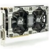 |
Inno3D GeForce GTX 670 iChill, Inno3D GeForce GTX 660 Ti Graphics Cards A couple of mid-range adapters with original cooling systems.
January 30, 2013 · Video cards: NVIDIA GPUs |
 |
Creative Sound Blaster X-Fi Surround 5.1 An external X-Fi solution in tests.
September 9, 2008 · Sound Cards |
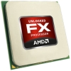 |
The first worthwhile Piledriver CPU.
September 11, 2012 · Processors: AMD |
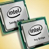 |
Consumed Power, Energy Consumption: Ivy Bridge vs. Sandy Bridge Trying out the new method.
September 18, 2012 · Processors: Intel |
| Latest Reviews | More RSS |
 |
Retested all graphics cards with the new drivers.
Oct 18, 2013 · 3Digests
|
|
Added new benchmarks: BioShock Infinite and Metro: Last Light.
Sep 06, 2013 · 3Digests
|
|
Added the test results of NVIDIA GeForce GTX 760 and AMD Radeon HD 7730.
Aug 05, 2013 · 3Digests
|
 |
Gainward GeForce GTX 650 Ti BOOST 2GB Golden Sample Graphics Card An excellent hybrid of GeForce GTX 650 Ti and GeForce GTX 660.
Jun 24, 2013 · Video cards: NVIDIA GPUs
|
|
Added the test results of NVIDIA GeForce GTX 770/780.
Jun 03, 2013 · 3Digests
|
| Latest News | More RSS |
Platform · Video · Multimedia · Mobile · Other || About us & Privacy policy · Twitter · Facebook
Copyright © Byrds Research & Publishing, Ltd., 1997–2011. All rights reserved.