 |
||
|
||
| ||
|
||
|
||
| ||
Non-Uniform Memory Architecture (NUMA) as a special type of memory organization in multi-processor AMD Opteron platforms has been existing for a long time already — one can say since the announcement of AMD Opteron 200 and 800 that support multi-processor configurations. But we still haven't carried out a low level analysis of its advantages and disadvantages. That'll be the subject of this article. Fortunately, our lab has a dual-processor system based on AMD Opteron CPUs. But at first let's revise the key features of this architecture. The majority of typical multi-processor systems are based on the symmetric multiprocessing architecture (SMP) that offers all processors a common FSB (and consequently a memory bus).  Simplified flowchart of an SMP system On the one hand, this architecture provides almost identical memory access latencies for any processor. But on the other hand, a common system bus is a potential bottleneck of the entire memory system in terms of no less important (and even much more important) bandwidth. Indeed, if a multi-threaded application is critical to memory bandwidth, its performance will be limited by this memory organization. What does AMD offer in its Non-Uniform Memory Architecture (its full name is Cache-Coherent Non-Uniform Memory Architecture, ccNUMA)? Everything is simple — as AMD64 processors have a built-in memory controller, each processor in a multi-processor system has its own local memory. Processors are connected between each other with HyperTransport that bears no direct relation to the memory system (which cannot be said about the traditional FSB). 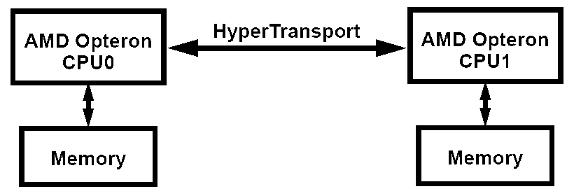 Simplified flowchart of a NUMA system In case of a NUMA system, processors experience low latencies for accessing local memory (especially compared to an SMP system). At the same time, remote memory (belonging to the other processor) is accessed at higher latencies. That's where the non-uniform memory organization notion originates from. But it's not hard to guess that if memory access is organized correctly (each processor operates with data solely in its local memory), such an architecture will have an advantage over a classic SMP solution due to no bandwidth limits of the common system bus. The total peak memory bandwidth in this case will equal the double bandwidth of the memory modules used. But the correct memory access organization is the key notion here. NUMA platforms must be supported both by OS (at least the operating system and applications should be able to "see" memory of all processors as a whole memory block) and by applications. The latest versions of Windows XP (SP2) and Windows Server 2003 fully support NUMA systems (Physical Address Extension must be enabled in 32bit versions (/PAE in boot.ini), which is fortunately enabled by default in AMD64 platforms, as it's required by Data Execution Prevention). What concerns applications, it first of all means that a program shouldn't deploy its data in the memory of one processor and then access it from the other processor. The effect of sticking to this recommendation or failing to comply with it will be reviewed now. Testbed configuration and software
Test ResultsThe tests were carried out in the standard mode for testing memory of any platform. We measured the following parameters: Average Real Memory Bandwidth for linear reading/writing from/to memory, Maximum Real Memory Bandwidth for Reading (Software Prefetch) and Writing (Non-Temporal Store), as well as Pseudo-Random and Random Memory Access Latency for Walking a 16MB data block. But the test method has been slightly modified: tests are now "tied" to a certain physical processor — this feature was implemented in RMMA long ago, but we had no time to try it. That's what it does: test data is always deployed by the first processor (for a NUMA-aware OS it means that this block will be deployed in the physical memory of the first processor). Then tests can be run on any processor available in the system. It helps evaluate the data exchange rate between a processor and memory (as well as other characteristics) — both local and remote, belonging to the other processor. Symmetric 2+2 mode, No Node InterleaveThere turned out a lot of BIOS memory settings in the dual processor system on AMD Opteron. To be more exact, at least three parameters are configured (Disabled/Enabled or Disabled/Auto), which gives us the total of 8 variants. They are: Node Interleave (memory interleaving between modes, that is integrated processor controllers — a nice feature to be reviewed below), Bank Interleave (classic interleaving of access to memory banks), as well as Memory Swizzle (similar to Bank Interleave, but still not quite clear :)). As changes of the last parameter had not effect on test results, we decided to leave it by default (Enabled). The other parameters varied. We used the symmetric 2+2 configuration in the first series of tests (two modules per each processor), Node Interleave was disabled, Bank Interleave varied between Disabled and Auto (the latter means that bank interleaving is according to the module characteristics).
Access to local memory (CPU 0) gives us quite a usual picture. Perhaps it even looks great, considering registered DDR-400 with timings far from being the fastest (3-3-3-8). Enabling Bank Interleave results in improving some memory bandwidth parameters (especially the average real memory write bandwidth, with the accompanying spread growth) and has practically no effect on latencies. When a processor accesses remote memory (CPU 1), it results in a noticeable deterioration of all memory characteristics. First of all it's a twofold drop of the maximum real memory read/write bandwidth (it's like a single-channel access mode, but the reasons of this limitation are not quite clear, as HyperTransport frequency in our case is 1000 MHz, which ensures the peak throughput of the interprocessor connection of 4.0 GB/s). Decrease of the average real memory bandwidth is less noticeable; latencies grow by 50-60%. Thus, the memory non-uniformity, mentioned in the theoretical section of this article, is evident (of course, not only in latency terms, but also in terms of memory bandwidth). It confirms the necessity of not only NUMA-aware OS, but also of specially optimized multi-threaded applications, where each thread independently allocates memory for its data and works with its memory area. Otherwise (single-threaded applications and multi-threaded ones, which don't care about the right data allocation in memory as far as NUMA is concerned) we should expect memory performance to decrease. Let's analyze this situation by the example of single-threaded applications, which are currently in majority. OS dispatcher in a multi-processor system shares CPU time for applications evenly between all the processors (thus, in case of a dual processor system, 50% fall on the first processor, and 50% — on the second). Thus, memory allocation must fall on one of processors (for example CPU0), while the application code, accessing the data, will run both on CPU0 and on CPU1. Memory system will operate at full efficiency only half of the time, it will operate at halved efficiency the rest of the time, as demonstrated by our tests. That's why, strange as it may seem, efficiency of memory operations in such applications can be increased by forcing them to one of processors (by specifying Process Affinity), which is actually easy to do. The situation grows worse in case of non-NUMA-optimized multi-threaded applications that also deploy their data in memory of only one of the processor. This configuration may be even outperformed by traditional SMP modifications — the total throughput will be limited by the throughput of one of the memory controllers; access latencies will be uneven. Nevertheless, even in this problematic situation, AMD version of NUMA provides for a way out; we shall describe it below... Asymmetric 4+0 modeAs for now, we decided... to "reduce the price" of the system — that is to imitate a predominant situation among cheaper dual-processor motherboards for AMD Opteron, when memory modules can be installed only for one processor — this memory is forced to become remote. Judging from theoretical assumptions, we cannot expect different results in this case — the only difference of this situation is that the "local" processor gets twice as much memory, while the "remote" processor still lacks it. So we publish them only to give a complete picture.
So it is — the theory is backed up by practice. Small differences can be seen only with enabled Bank Interleave — in this case the memory bandwidth goes down a little and its spread grows (such a large spread has to do with gradual increase of memory write bandwidth, when the block is incremented from 4 MB to 16 MB). It's not very important in our analysis though, as it reflects only internal peculiarities of Bank Interleave with two or four certain memory modules. Let's ask a more important question: do our results mean that we can use the cheaper memory organization? You certainly shouldn't do it, both in case of NUMA-optimized applications and without them. In the first case the reason is clear — well optimized multi-threaded applications, if they are critical to memory bandwidth, get maximum from the symmetric memory organization. In the second case, the symmetric 2+2 organization (instead of the asymmetric 4+0 mode) allows Node Interleave... or just profits from the correct application assignments to processors. Symmetric 2+2 mode, Node InterleaveThis is finally the most interesting moment — a solution for regular NUMA-unaware applications. It's essentially very simple: to interleave memory by 4KB pages between the modules in different nodes (memory controllers). In case of a dual processor system one can say that all even pages fall to the first processor, while all the odd pages belong to the second. So, irregardless of what processor deploys data in memory, the data will be evenly shared between the memories of both processors. Irregardless of what processor executes code, half of memory accesses will refer to local memory, and the other half — to remote memory. Well, let's see how it works in practice.
Full symmetry in all parameters, there is no non-uniformity to be seen! Memory access latencies are truly average (for example, pseudo-random access: (45 + 70) / 2 = 57.5 ns). The situation with memory bandwidth is worse — we can see only 4.2 MB/s instead of the expected theoretical value (6.4 + 3.2 / 2) = 4.8 MB/s. But approximately the same values would have been obtained even without Node Interleave — for a simple single-threaded application, which is not tied to a certain processor. Moreover, as we have already said above, forcing an application to be executed by a selected processor even allows to increase memory bandwidth and reduce latencies. Thus, the only adequate usage for Node Interleave is just for non-optimized multi-threaded applications, which will otherwise be limited by the memory bandwidth of one of the memory controllers. ConclusionIn conclusion, let's briefly analyze all possible variants — platforms, equipped with dual channel DDR-400 (in fact, we can just as well speak of dual channel DDR2-400, -533, -667, etc, if you keep in mind that a 200 MHz FSB still limits the memory bandwidth at 6.4 GB/s) and applications — single-threaded (one or several) and multi-threaded (regular and NUMA-optimized).
*in case the application is tied to one of processors So, SMP systems (dual processor Intel Xeon, as well as... any existing dual core processors) — the theoretical memory bandwidth is always limited to 6.4 GB/s, it's a peak bandwidth of the one and only FSB. Inexpensive asymmetric NUMA systems don't look much better, sometimes they are even worse than traditional SMP systems. They are worse in case of single-threaded applications, if they are not tied to the processor with memory. Peak memory bandwidth in any other cases is also limited to 6.4 GB/s — bandwidth of the only available memory interface. Symmetric NUMA systems almost always have an advantage over SMP as well as over asymmetric NUMA systems. The peak memory bandwidth of 12.8 GB/s on such platforms can be reached either by special NUMA-optimized applications, or... by two regular single-threaded applications, each one assigned to its own processor. And finally, what does Node Interleave give to symmetric NUMA platforms? We can see the advantage only in one case — with non-optimized multi-threaded applications (provided that each of the threads intensively operates with the data from memory). If single-threaded applications are started correctly, or if NUMA-optimized applications are used, this mode certainly shouldn't be enabled, it may only spoil the performance. Thus, drawing a conclusion from our analysis: NUMA is certainly a more perfect memory architecture compared to traditional SMP solutions. In most cases it provides advantage over such systems in terms of low level memory characteristics. Write a comment below. No registration needed!
|
Platform · Video · Multimedia · Mobile · Other || About us & Privacy policy · Twitter · Facebook Copyright © Byrds Research & Publishing, Ltd., 1997–2011. All rights reserved. | |||||||||||||||||||||||||||||||||||||||||||||||||||||||||||||||||||||||||||||||||||||||||||||||||||||||||||||||||||||||||||||||||||||||||||||||||||||||||||||||||||||||||||||||||||||||||||||||||||||||||||||||||||