 |
||
|
||
| ||
|
||
|
||
| ||
 Contents
Beginning of autumn... As it had already been five years ago with a loud announcement of the first video card with T&L hardware support (GeForce256), today we meet new products from NVIDIA. Of course they do not belong to High-End, but their announcement is no less interesting. The announcement has been actually made before, in August, but it provided only video cards' features. And now, as many other mass media, we have a chance to highlight the features of the newest Middle End 3D accelerators.
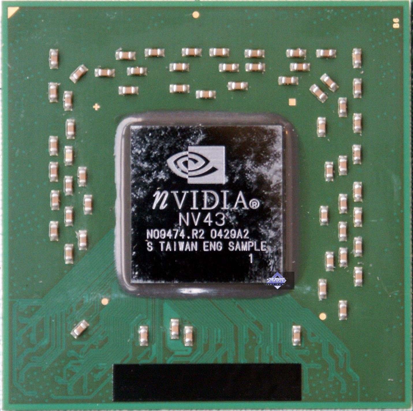
Up to recently this market segment has been dominated by ATI products: RADEON 9600/PRO/XT, X600PRO/XT outscoring its competitors NVIDIA GeForce FX 5700/Ultra, PCX5750/5900 by their performance in modern games with active shader usage. And only FX 5900XT, drawn down from "above" into this sector, managed to become popular and to press the supremacy of the canadian products. And now... "Nalu is on the way to the first prize... Ruby will have to hold the line..." Yes, the mermaid and the valiant girl from the corresponding NVIDIA and ATI demos, demonstrating the new technologies (SM3.0 from NVIDIA and 3Dc/SM2.0b from ATI) are not selected as our heroines by chance. The new products from the californian company, which will be reviewed today, completely support shaders v3.0, as their elder brothers. Will Ruby let catching her up Nalu have her king diamond? The new announcements from ATI in the same video cards' sector are round the corner. What will be the outcome of this battle? - We don't know yet. I think that the article about RV410 will be no less interesting and gripping. But for now we'll put aside these issues and examine NV43 (GeForce 6600GT/6600) as if these cards are already on sale. Correspondingly, their competitors will be presently popular accelerators within the 150-200 USD price range. And of course predecessors of these new video cards. Running a few steps forward, I want to note that NV43 has built-in support for the PCI-Express interface (or PCX), that's why AGP products without HSI bridge are impossible. Thus, they will be costlier to manufacture and will be launched later than their PCX counterparts (if they will be launched – it'll be all up to the demand). It's a considerable shortcoming of the new products today, because PCX sector has just started to evolve and the demand for such platforms is minimal for now. That's why, no matter how wonderful the new product is, it is doomed to little retail demand from the very beginning, because benefits from the AGP to PCX upgrade are doubtful so far. On the other hand, OEM market and PC assemblers, especially foreign ones, will not fail to launch models with not so expensive (as top models) but still meeting modern requirements DirectX PCX solutions. Besides, who knows, perhaps the launch of interesting and profitable in terms of price-performance video cards will whip up the interest to PCX on the whole. So, time will show. And don't forget that ATI will launch its RV410 with native support for PCX only, and the canadian company does not have its own bidirectional bridges AGP<->PCX. So it will hardly be able to implement its new products on the AGP bus. However, this sector is overcrowded anyway, and there are a lot of solutions similar in performance, which had been manufactured before or are produced now. It was very interesting for us to compare not only video cards on the same interface, but also AGP and PCX implementations. Of course it's difficult to do, because the platforms differ considerably. However we remember that we are in Middle End sector, where modern processors are quite capable of loading accelerators by 100%, and after a certain resolution barrier the performance is not so platform-dependent. Below are the results of our cross-platform research. And now let's return to the objects of today's analysis: NVIDIA NV43 or GeForce 6600GT/6600 (the series now contains two video cards, which differ only by parts).
Official specifications on GeForce 6600GT/6600 (NV43)
GeForce 6600 GT, specification of the reference card
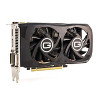
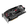
A list of existing cards based on NV43:
Chip architecture
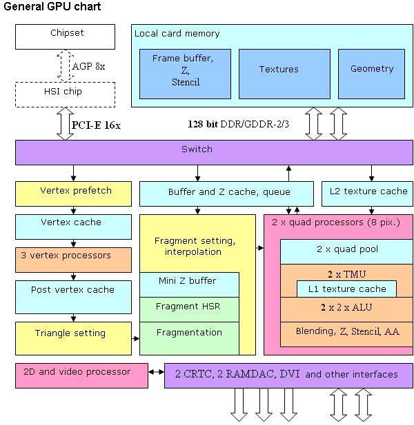 We didn't find any special architectural differences from NV40, which is not surprising – NV43 is a scaled (by means of reducing vertex and pixel processors and memory controller channels) solution based on the NV40 architecture. The differences are quantitative (bold elements on the diagram) but not qualitative – from the architectural point of view the chip remains practically unchanged. Thus, we have 3 (there were 6) vertex processors and two (there were 4) independent pixel processors, each working with one quad (2x2 pixel fragment). It's interesting, that this time PCI Express has become a native (i.e. on-chip) bus interface, and AGP 8x cards will have an additional bidirectional PIC-E <-> AGP bridge (shown with dotted line), which has been already described. The architecture of vertex and pixel processors and of the video processor remained the same – these elements were described in detail in our review of GeForce 6800 Ultra (link). And now let's consider potential quantitative and qualitative changes relative to NV40: Theoretical considerations about what and how has been cut downOn the whole, at present we have the following series of solutions based on NV4X and R4XX:
*) the data is based on unverified rumours (beyond3d forum and other unofficial web resources), these products will soon be announced officially. While 6800 Ultra, GT and just 6800 look rather balanced in terms of memory band and fill rate, 6800LE will often experience the insufficient fill rate - memory band is excessive, and both 6600 models will first of all suffer from insufficient passband. Peak fill rate in 6600 GT is almost 2/3 of fill rate in 6800 Ultra, while its memory bandwidth is twice as low (without taking into account potentially reduced caches and two-channel memory controller). Thus we can predict that the weak point in the 6600 series will be high resolutions and full-screen antialiasing modes, especially in simple applications. And the strong point – programs with long and complex shaders and anisotropic filtering without simultaneous MSAA. We'll check this assumption later in game and synthetic tests. It's difficult to judge now how reasonable the introduction of 128-bit memory bus was - on the one hand, it cheapens chip packaging and reduces a number of defective chips, on the other hand, the cost difference between 256-bit and 128-bit PCBs is small and is excessively compensated by the cost difference between usual DDR and still expensive high-speed GDDR3 memory. Perhaps, from the manufacturers' point of view the solution with 256-bit bus would be more convenient, at least if they had a choice. But from the point of view of NVIDIA, who manufactures chips, very often selling them together with memory, the 128-bit solution with GDDR3 is more profitable. Its impact on performance is another story, the potential restriction of excellent chip features because of the considerably reduced memory passband is obvious (8 pipelines, 500 MHz core frequency, and that's not the limit yet).
This fact is especially troubling on the background of rumours about the seniour X700 model, which will be equipped with 256-bit memory. However, note that the Ultra suffix is still reserved by NVIDIA – considering a great overclocking potential of the 110 nm process, we can expect a video card with the core frequency at about 600 MHz or less, 1100 or even 1200 (in future) memory and with the name 6600 Ultra. The question is how much it will be? In far-reaching perspective, we can forecast a launch of a renewed 256-bit variant of the mainstream solution, let's call it NV46, optimized by performance, with 8 or even 12 pipelines and a 256-bit bus. To all appearances, vertex and pixel processors in NV43 remained the same, but the internal caches could be reduced proportionally to the number of pipelines. However, the number of transistors does not give cause for trouble. Considering not so large cache sizes, it would be more reasonable to leave them as they were in NV40, thus compensating for the noticeable scarcity of memory passband. It's quite possible that the ALU array, which contains rather large quantities of transistors responsible for postprocessing, verification, Z generation, and pixel blending to write the results to frame buffer, was also reduced in each pipeline relative to NV40. The reduced memory band will not allow to write 4 full gigapixels per second anyway, and the fill rate potential (8 pipelines for 500 MHz) will be validly used only with more or less complex shaders with more than 2 textures and corresponding shader calculations. We'll check all these assumptions in the course of our synthetic and game tests.
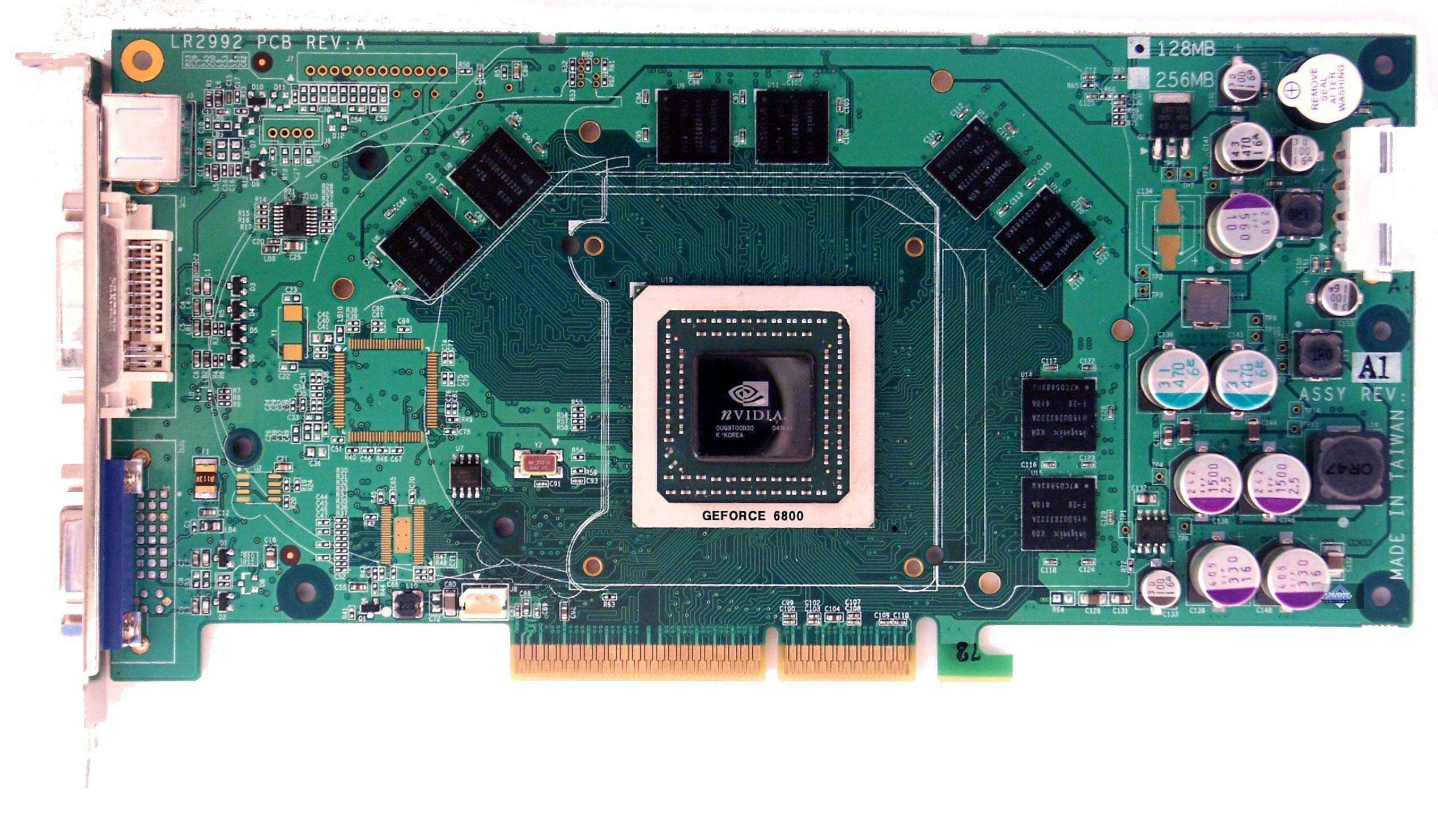
 Before examining the card itself, we'll publish a list of articles devoted to the analysis of the previous products: NV40/R420. It's obvious already that the NV43 architecture is a direct heir to NV40 (its chip capacity was halved).
Theoretical materials and reviews of video cards, which concern functional properties of the GPU
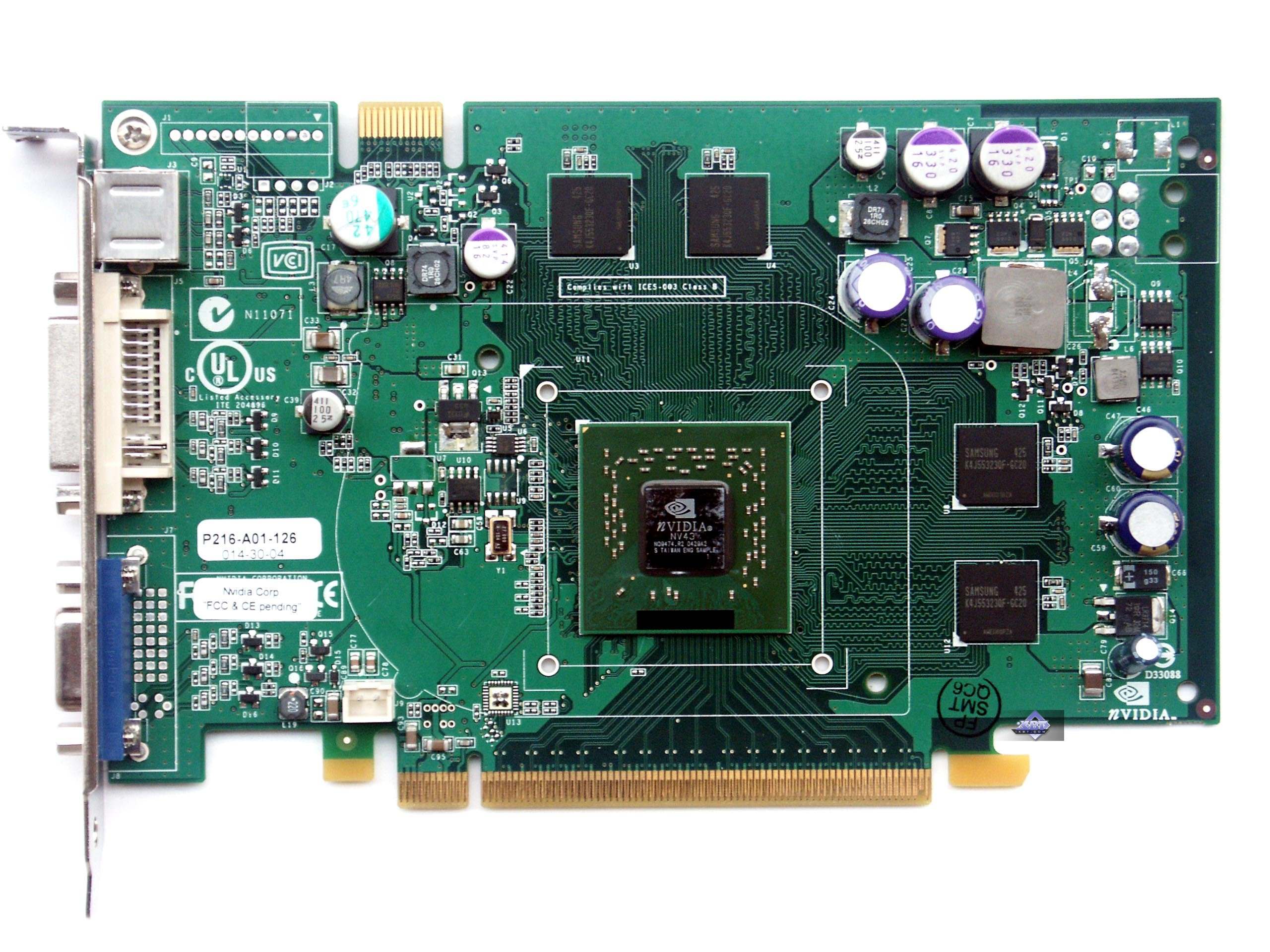
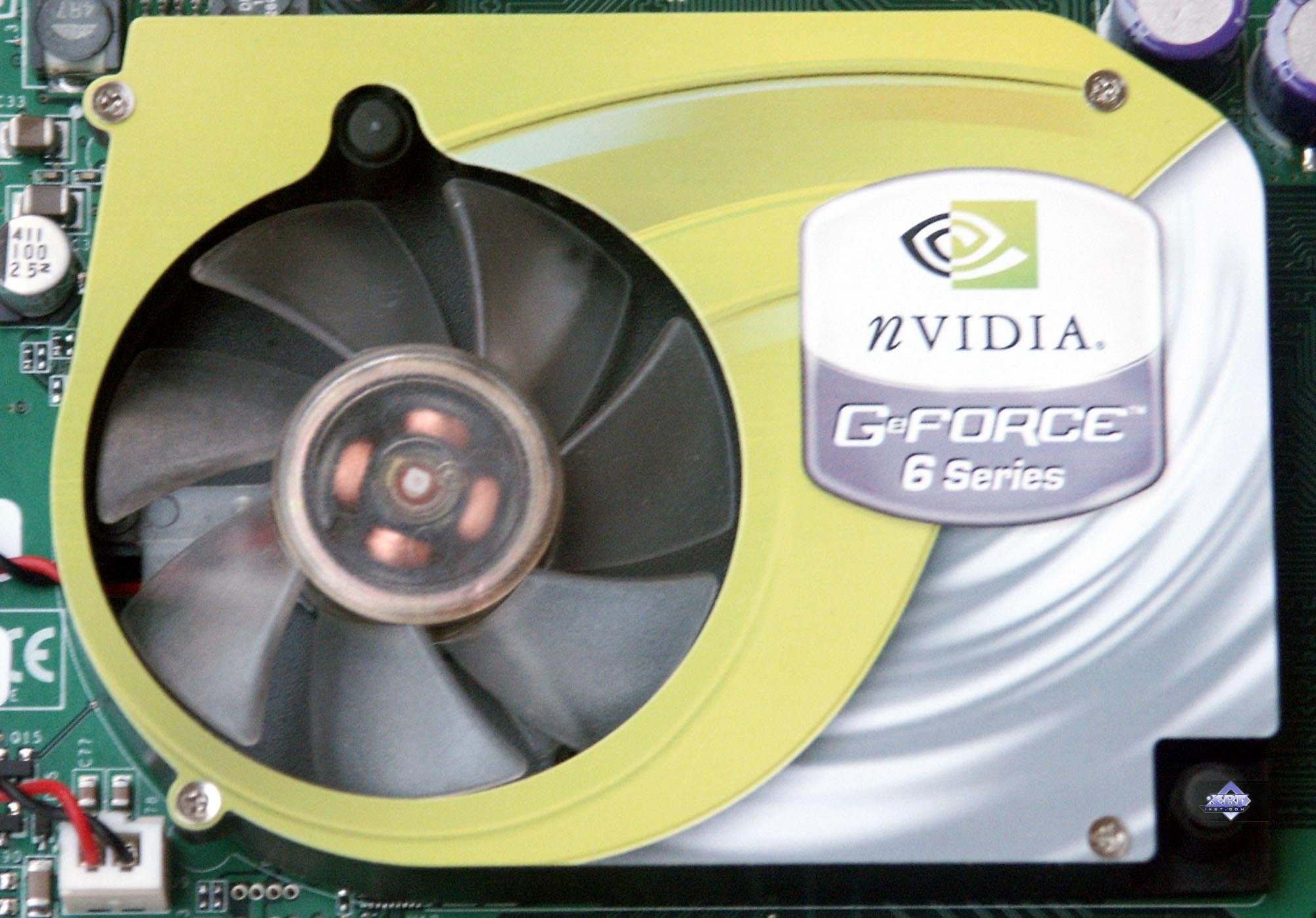
I repeat that this is only the first part of the review devoted to the performance of the new video cards. The qualitative components will be examined later in the second part (3D quality and video playback). Now about the video card. Why do we mention two video cards in the title and actually review only one? - The fact is, 6600GT and 6600 differ only by operating frequencies, that's why we can emulate GF 6600 with high probability by reducing 6600GT frequencies. That's what we did. Taking into account that production GeForce 6600 cards will be equipped with common DDR instead of GDDR3 (besides frequencies, they have different timings) and that NVIDIA does not declare strict memory operating frequencies for such video cards, and there may be memory clocks from 250 to 300 MHz, we cannot obviously speak about 100% match of our results with those demonstrated by final GeForce 6600. But we can reckon. It's even useful. That's why we'll include GeForce 6600 300/300 (600) MHz into our results (an extreme case). It's clear to everybody that real 6600 will demonstrate the performance NOT HIGHER than that on our diagrams, and we can reckon the range. So, reference card GeForce 6600GT. Video card
GF 6600GT design is obviously unique, it is not similar to any previous design. First of all, this is due to the reduction of PCB dimensions allowed by the lack of 256-bit bus, which actually influences PCB dimensions. And a critical simplification of the power block provided for the PCB area reduction (all PCX card consuming less than 75W do not require external power, and it simplifies the design). Our object consumes less than 75W even at maximum load, so there is no need to connect it directly to the power supply unit.
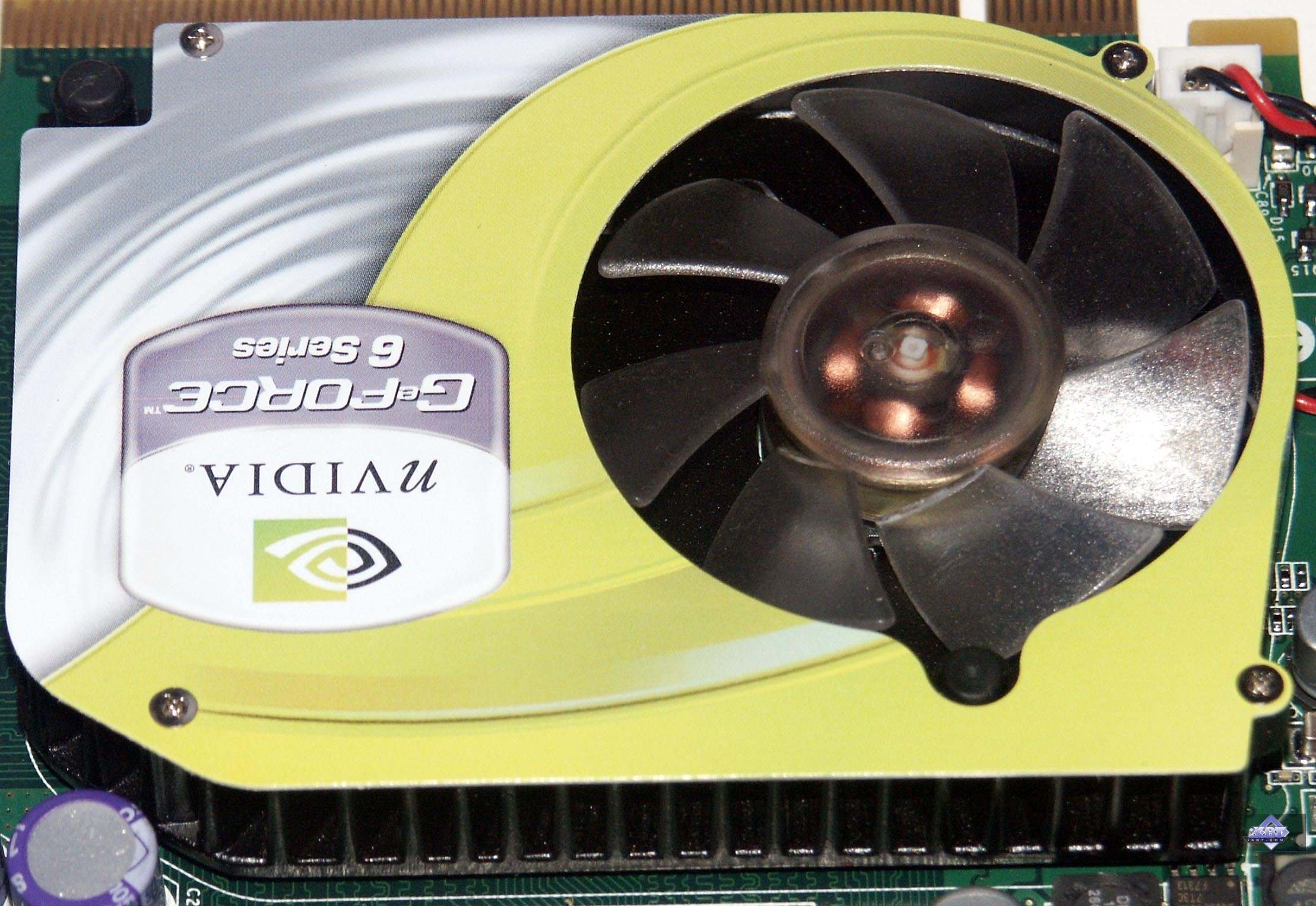
Despite enormous frequencies for an 8-pipeline chip, the cooler is rather primitive.
GPU location is relatively small (it's quite clear, 128-bit but), it looks like GeForce FX 5700. The chip size is also almost the same. But while NV36 contained only 4 pixel and 3 vertex pipelines with this dimensions, in this case it contains twice as many pixel pipelines. 0.11 micron process...
This video card has an important feature, designed for the future, namely the SLI support (that is, as in times of Voodoo2, there is an opportunity to increase the total capacity of 3D graphics by an additional similar accelerator). For this purpose the upper part of the card contains a corresponding connector for a special cable to two video cards to synchronize their operation: 
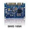
To finish the examination of the card, note that it has the VIVO support implemented with Philips 7115 (we haven't come across this codec yet, so our permanent researcher of multimedia add-ins and features of video cards Alexei Samsonov is looking forward to test the new card, so wait for an article concerning this issue). 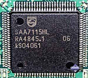
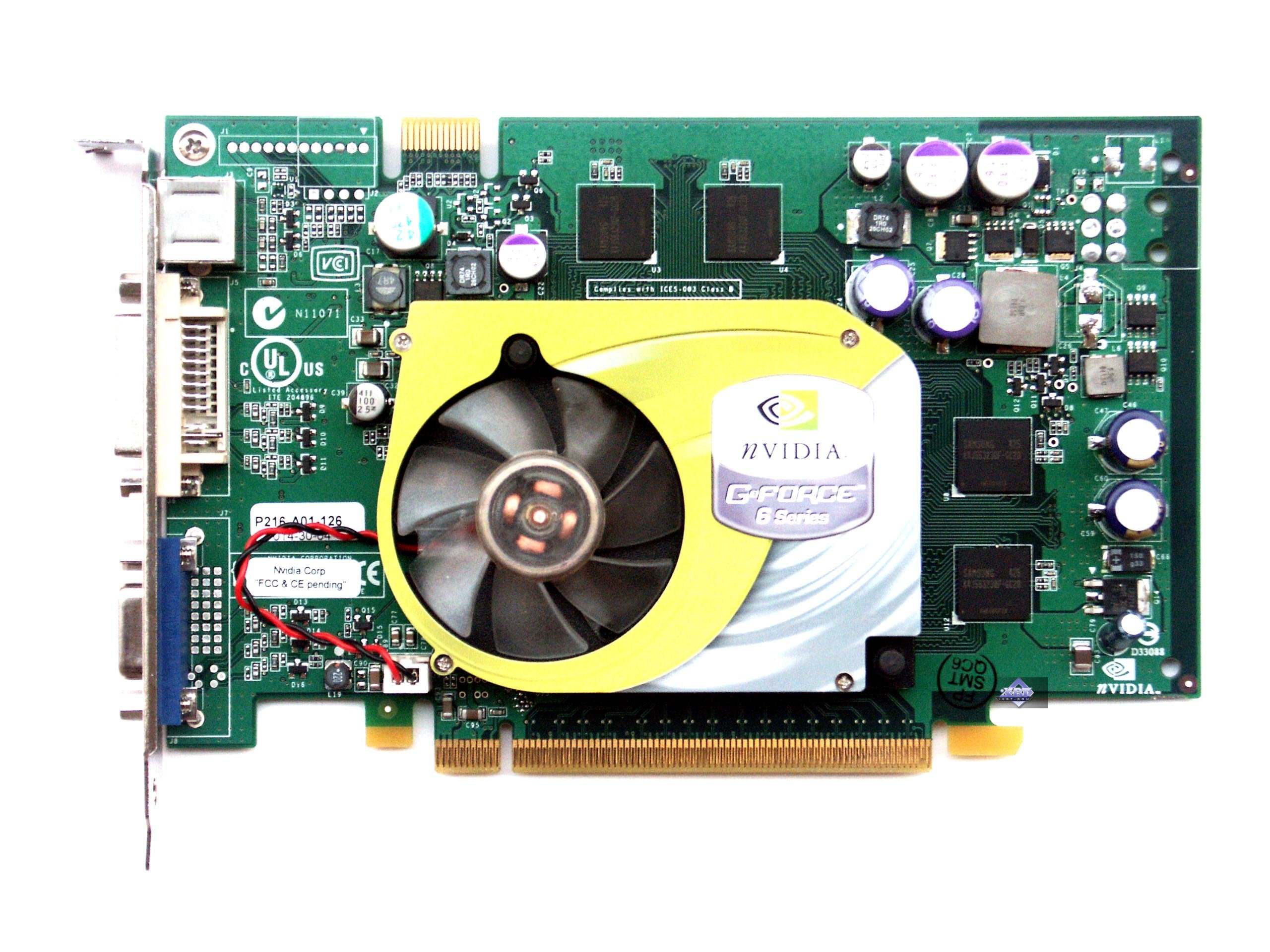
Now what concerns overclocking. Thanks to responsiveness of Alexei Nikolaychuk (author of RivaTuner) this utility is already compatible with NV43. 
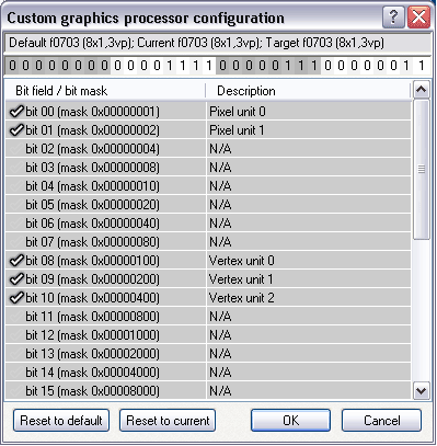 The number of pipelines in this card (both pixel and vertex) can be detected. On the second screenshot you can see that two quads (four pixel pipelines) operate in this card. So, the card operated steadily at 590/590 (1180) MHz!. Unprecedented potential! I can even assume that after the launch of ATI RV410, NVIDIA will launch GeForce 6600 Ultra (that's the reason for the seniour model presently bearing only the GT suffix).
At these frequencies the card worked with an external cooler. Here are the temperatures we registered:  Yes, sometimes the core heated to 88 degrees, but as you know, this is not the limit for these chips (they can heat up to 100 degrees). It's interesting to note that the external cooler actually cooled only memory, because its removal did not lead to any core temperature rise.
And here is what we see at regular frequencies: 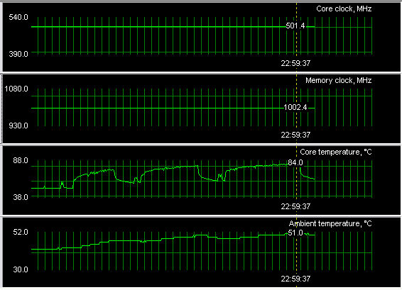
[ The next part (2) ]
Write a comment below. No registration needed!
|
Platform · Video · Multimedia · Mobile · Other || About us & Privacy policy · Twitter · Facebook Copyright © Byrds Research & Publishing, Ltd., 1997–2011. All rights reserved. | ||||||||||||||||||||||||||||||||||||||||||||||||||||||||||||||||||||||||||||||||||||||||||||||||||||||||||||||||||||||||||||||||||||||||||||||||||||||||||||||||||||||||||