As part of regular Russian Intel Developer Forum held in Moscow on October 19-20, along with the general presentation of new Intel semiconductor technologies Josh Walden presented a separate technical report entitled "Intel's 65 nm Logic Technology: Continuing Moore's Law in a Power Limited World". The lecturer, head of the Fab24 laboratory located in Leixlip, Ireland, acquainted its audience with the current state of affairs in Intel in the field of semiconductor technologies and gave an account of the corporative plans for the nearest future, which included designing and launching microprocessors based on the 65nm process technology in 2005, which has been already used today in pilot SRAM memory chips comprising over 0.5 billion transistors manufactured on 300mm wafers. We shall give a detailed account and analyze the main technical moments, which were presented in this report, and digress into the nearest future of the semiconductor technologies of the corporation.
Current state of affairs of Intel semiconductor technologies: 90nm process technology
First of all let's dwell on the current state of affairs in the corporation in the area of semiconductor and microprocessor technologies, because the new 65nm process technology is in many respects a development of the ideas laid in foundation of the current generation of 90nm microprocessors. So, let's enumerate the key points of the modern 90nm process technology.
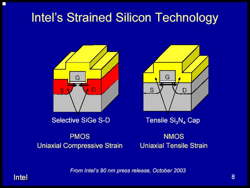
1. Strained silicon technology
These days it's probably the most famous "en masse" technology, which distinguishes Intel 90nm process technology from previous ones. It solves one of the most important tasks of the microprocessor industry – to increase performance of transistors forming a processor core. The essence of this technology is in tensile (in case of NMOS transistors) or compressive (PMOS transistors) silicon lattice (unipolar transistor channel material) resulting in increased electron-hole conductivity, that is accelerated current via the channel due to its reduced resistance (up to 30% in PMOS transistors and up to 10% in NMOS transistors). In its turn, it leads to increased switching speed of transistors, finally resulting in increased CPU clock frequency capacity (taking into account that the microprocessor core is a CMOS solution, that is a combination of PMOS and NMOS transistors, the average performance gain can be expected to be up to 20%). The regular silicon lattice is "strained" when stretched or compressed, which is reflected in the name of this technology.
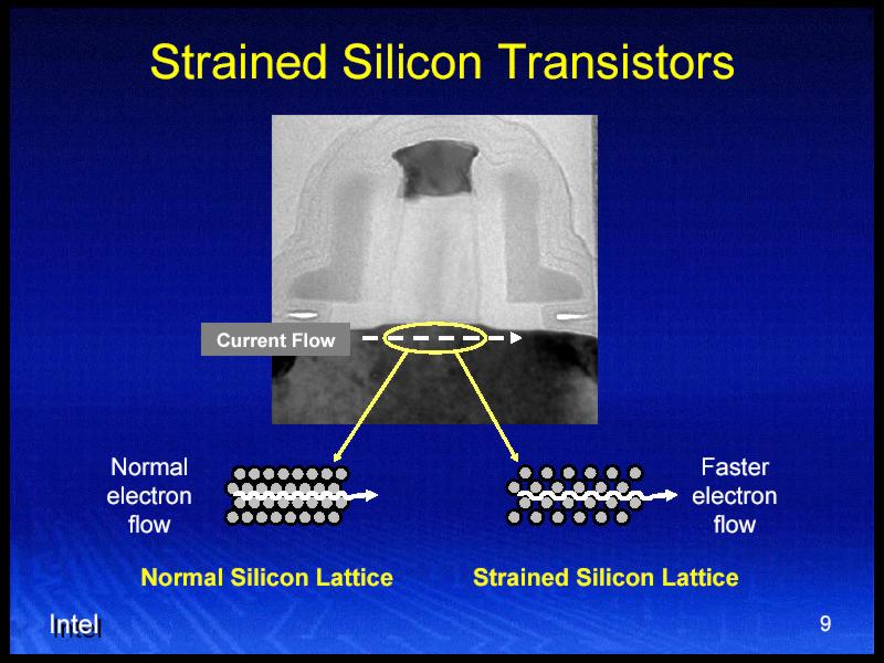
Strained silicon technology from Intel. On the left – compressive silicon lattice of PMOS transistors and tensile silicon lattice of NMOS transistors; on the right – currents through the regular and strained silicon lattices.
2. Improved transistors
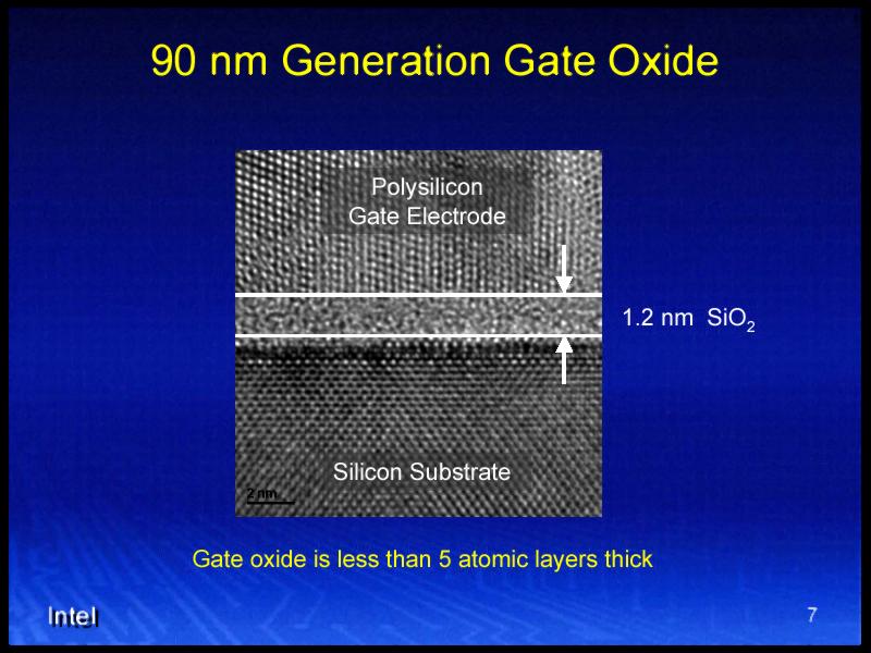
The essential constituent of Intel's 90nm process technology is the use of miniature, high-performance transistors with low power consumption operating at reduced voltage (~1.2 V). Transistors are characterized by the 50nm thickness of the gate made of polycrystalline silicon coated with Nickel Silicide (NiSi) – this material has lower linear electrical resistance than the previously used cobalt disilicide (CoSi2) in gate lengths below 100nm. Gate oxide thickness in 90nm transistors is held at 1.2 nm. The latter is made of regular silicon dioxide (SiO2), which has performed very well for the last 30 years as material for this transistor component due to its manufacturing simplicity (the oxide layer is manufactured "in place", that is in the process of transistor manufacturing by thermal oxidation of the substrate surface). Besides, this material provides an opportunity to further increase transistor performance by means of reducing the thickness of the insulating layer formed (of course to a certain limit, we'll cover this topic below).
90nm transistors. On the left – general view of the transistors; on the right – gate oxide.
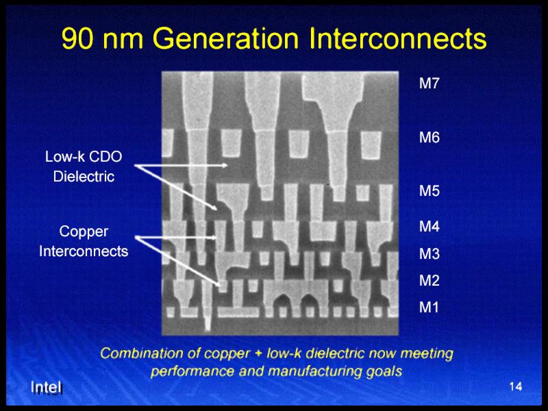
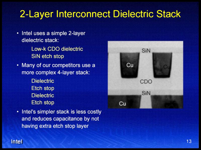
3. 7-layer transistor interconnects
The current process technology includes the usage of 7-layer copper interconnects of high density resulting in reduced total product costs as well as a new dielectric type with low-k, being silicon nitride (SiN) combined with some carbon-doped oxide (CDO) material (exact composition is not disclosed). This allows to reduce the "interconnect" capacitance by 18-20% in comparison with silicon oxyfluorade (SiOF) used in the 130nm process technology, which provides improved performance and lower chip power.
90nm transistor interconnects. On the left – general view of the interconnects, on the right – dielectric layer structure.
4. 300 mm wafer fabs
To manufacture 90nm chips, Intel uses only 300 mm wafers, which are manufactured on the three largest 300 mm fabs on a mass scale: D1C in Hillsboro, Oregon, F11X in Albuquerque, New Mexico, and F24 in Leixlip, Ireland. The chips are manufactured using «Copy Exactly!» methodology for matched yield and performance. The main benefit is a result of the die-wafer dimensions relation, which is reduced approximately by 2.5 when switching from the 130nm process technology on 200mm wafers to the 90nm technology on 300mm wafers. Besides the economic benefits, the 300mm manufacturing is safer for environment due to the same relation.
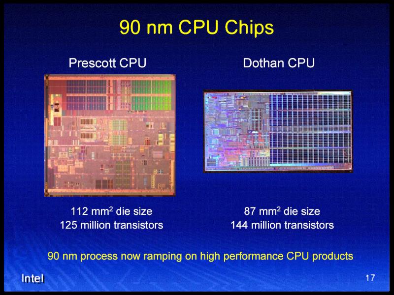
So, we have considered the main points that distinguish the modern 90nm process technology from the previous ones and allow higher performance of the final product, on the one hand, and higher economic profitability and environmental safety of manufacturing, on the other hand. In conclusion I want to note that the process technology under review has been successfully implemented in Prescott and Dothan processor cores, announced by Intel on February 2 and May 10 2004 correspondingly.
90nm Processors in Production.
The nearest future of the semiconductor technologies from Intel: 65nm process technology
Having reviewed the current state of affairs in the industry, it'll be only logical to proceed to the new 65nm process technology, which has been already demonstrated in 70Mbit pilot samples of cache memory with 0.57 µm2 SRAM cells to be put into production in 2005. As always, we'll start with the key points, which are essentially similar to the 90nm process technology points we have just reviewed above. Nevertheless, it's important to note that the information below is of somewhat "preliminary" character, because more information on Intel's 65nm logic technology will be presented in about 1.5 months at the IEEE International Electron Devices Meeting in San Francisco Dec. 12-15 2004.
1. Improved strained silicon technology
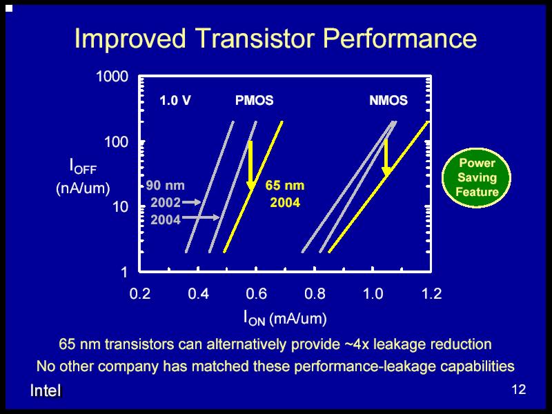
Strained silicon technology, which Intel has used starting from the 90nm process technology reviewed above, gets its further development in the 65nm process technology. Enhanced strained silicon technology provides the new process technology with still higher switching speed of the transistors due to increased by 10-15% drive current (ID, or ION) at practically constant leakage current via the gate oxide layer (IGate). According to Intel, the advanced silicon strain technology of the second generation will raise the clock frequency by 30% (in comparison with "non-strain" silicon).
2. New 65nm transistors
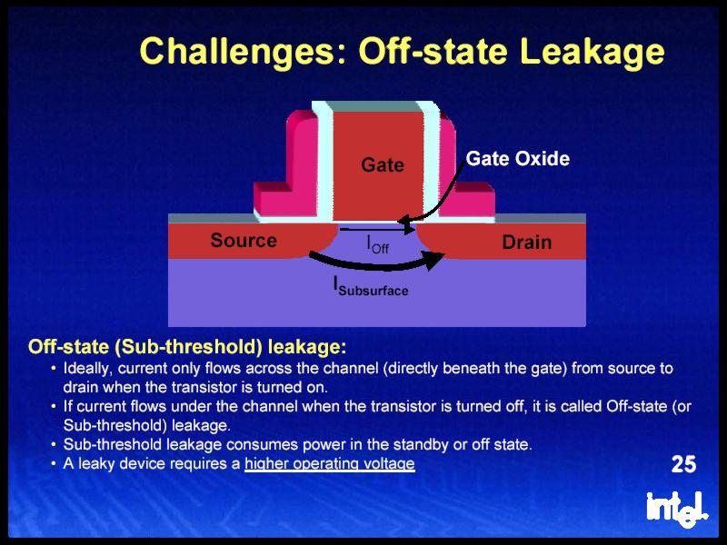
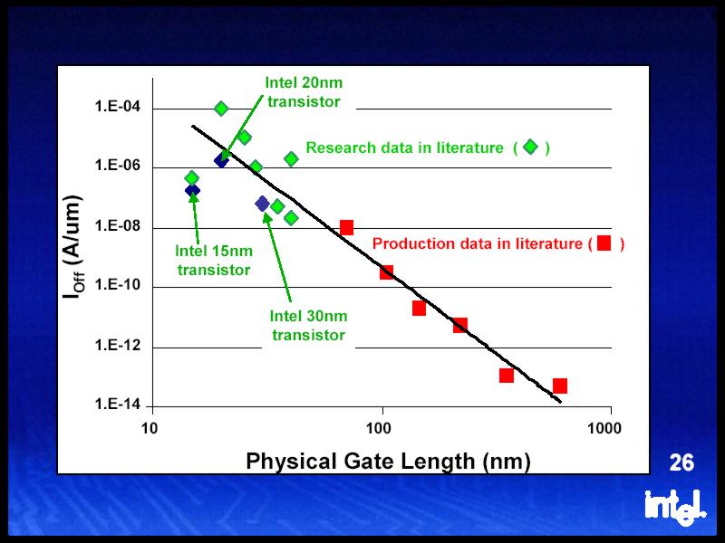
65nm transistors are characterized by further reduced nickel silicicated polysilicon gate length to 35 nm at the retained gate oxide thickness of 1.2nm. The latter factor helps preserve the leakage current at the same level, and the combination of these factors reduces gate capacitance (CGate) to 20%, which reduces chip active power. Nevertheless, we shouldn't forget about such an important characteristic of a field transistor as off-state current (IOFF) – the current flowing from the source junction to the drain junction of the transistor when it is turned off, which is induced by partial breakdown of the gate material as well as of the wafer material. The newest presentation of the 65nm process technology makes no mentions of this fundamental issue. To be more exact, IOFF is to all appearances subtly substituted for IGate! But it's well known from literature that the reduction of gate length will inevitably increase IOFF, which is not denied by Intel in several other presentations, by the way.
The problem of current leakage in off mode (IOFF). On top – explanation on the essence of the problem. Below – ION / IOFF ratio for 90nm and 65nm transistors according to the latest presentation of the 65nm process technology (on the left) and the dependence of IOFF on the gate length according to the presentation of "future transistors" from Intel (on the right). There are obvious IOFF inconsistencies between two different presentations from the same company.
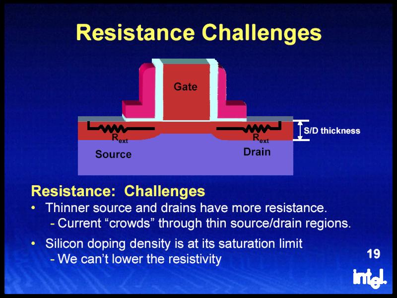
Out of additional new features implemented in 65nm transistors, first of all we should note their voltage reduced to 1.0 V, which has a positive effect on the dissipated power. What concerns materials, the new process technology completely switched to nickel silicide (NiSi) as a common material both for transistor gate coating as well as source and drain coating, which results in reduced electrical resistance of the latter and to additional reduction of power consumption. At last, the contacted gate pitch in the new process technology is reduced to 220 nm for higher density of chip elements.
The problem of increased source-drain material resistance at smaller dimensions. Solution to the problem in the 65nm process technology – nickel silicide (NiSi) used for coating these transistor components as well as for gate coating.
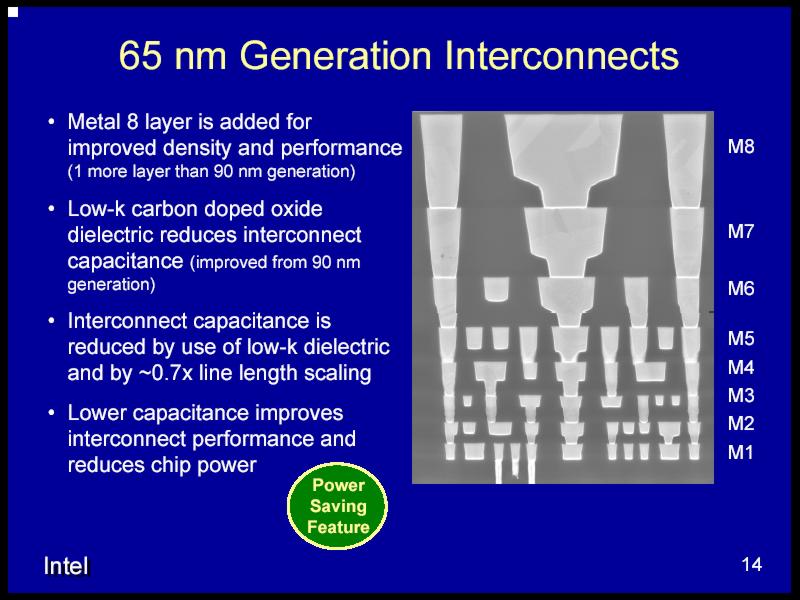
3. 8-layer transistor interconnects
The new process technology also introduces changes into the interconnect manufacturing scheme. First of all, another (the 8th) metal (copper) layer is added for improved density of contacts and higher propagation speed of electric signals. Low-k carbon doped (CDO) oxide is still used as dielectric, but its manufacturing technology is noted to be improved from 90nm generation. This new material together with the new method of 0.7x line length scaling of copper interconnects result in further reduction of interconnect capacitance, which leads to reduced chip power dissipated at transistor interconnects, as already noted in the previous chapter.
65nm transistor interconnects. General view and brief description of their manufacturing technique.
4. 0.57µm2 SRAM cells, sleep transistors
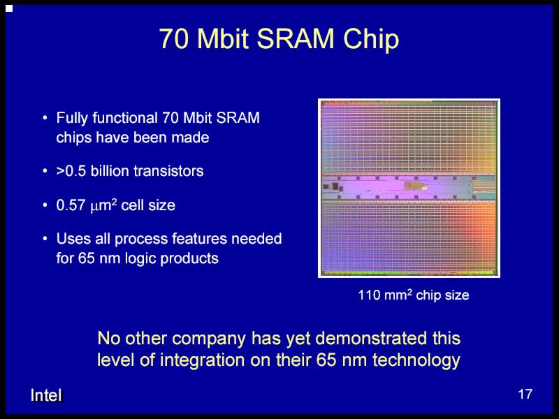
65nm process technology in manufacturing 4 Mbit SRAM chips was first announced by Intel in November 2003. Later on, the company managed to produce fully functional 70 Mbit SRAM chips by this process technology, which had a comparatively small die area – 110 mm2. Manufacturing SRAM chips with small area and high capacity is obviously essential to integrate large volumes of cache memory into a processor core, which in most cases has a positive effect on performance of the final product in real applications.
65nm SRAM chips. On the left – view of the chip and its specification; on the right – power saving properties of the chip due to sleep transistors
65nm SRAM chip cell packs six transistors (6T technology) in an area of 0.57 µm2 (for comparison, the area of a 6T cell in 90nm SRAM cache is 1.0 µm2) and is characterized by a relatively low static noise margin (SNM), which allows to operate at voltages of up to 0.7 V.
As is noted in the presentation of the 65nm process technology, an important distinction of the new 65nm SRAM chips is the usage of so called sleep transistors, which control the current flow to SRAM Cache sub-blocks depending on their state (sleep transistors shut off leakage in inactive sub-blocks, and cut it in when any of the elements of the array is accessed). The use of sleep transistors obviously results in considerable SRAM cache leakage reduction, which is especially important for mobile devices. Though this technology is considered a distinctive feature of 65nm SRAM devices, we should note that a similar (we do not contend that it's the same) technology has been actually implemented and used since 130nm Pentium M mobile processors with Banias core, capable of putting to sleep inactive parts of L2 cache.
5. 300 mm wafer fabs
65nm chip production involves the same 300mm wafers that are used in manufacturing the current generation of 90nm processor cores. Pilot production of 65nm devices is currently running in D1D fab in Hillsboro, Oregon, where this process had been developed.
Major tasks for the nearest future of Intel's semiconductor technologies
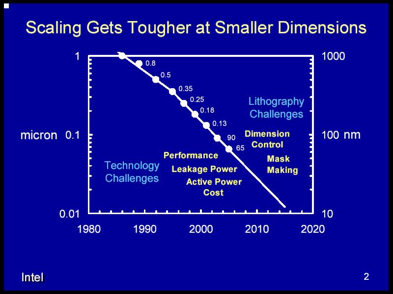
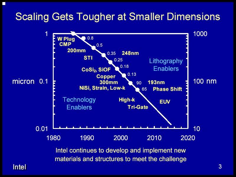
Having reviewed the 65nm process technology conceived by Intel corporation, let's proceed to a more general analysis of technological problems and tasks, which must be solved to realize this and subsequent, still "smaller" in terms of transistor dimensions, processes. It's not for nothing that the presentation of the 65nm process technology held at IDF 2004 Russia could have been opened with the slogan "Scaling gets tougher at smaller dimensions". Tasks and their solutions can be divided into two categories – technological and lithographic.
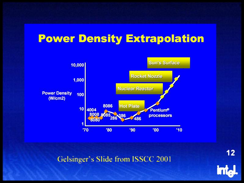
Technological tasks of the future semiconductor technologies from Intel and their solutions (on top). Increasing power density of microprocessors as the process technology progresses (below) is just an interesting analogy between hot plates, nuclear reactors, rocket nozzles, and Sun's surface, which the author found by chance in one of Intel's presentations...
Technological tasks
What are the major technological tasks of the future semiconductor technologies? Among the most important Intel notes the following: performance (obviously meaning the increasing difficulty of "frequency built-up" or "Gigahertz race" the company likes so much), the problem of leakage current reduction and the "costs" of further increase of effective output (increase of the ION / IOFF ratio).
| Transistor dimensions |
Problems |
Solutions |
| 90-65 nm |
Performance |
Strained silicon, nickel silicide
(NiSi), low-k dielectric (CDO) for interconnects |
| 65-45 nm |
Leakage current |
high-k dielectric for a gate insulating
layer |
| 45-30 nm |
Effective output |
Tri-gate transistors |
On the table above you can see that the performance problem, which
is referred to 90-65nm process technologies, can be considered solved:
present and future microprocessors successfully use and will use silicon
"strain", nickel silicide for gate coating (as well as source-drains
coating), CDO dielectric with low-k to isolate copper interconnects
and reduce interconnect capacitance. In this connection, it'll be
more interesting to dwell on the second problem, which refers to not
so distant a future – leakage current problem. And let's defer
the problem of effective output and tri-gate transistor technology
for our future articles on this issue.
Problem of leakage current
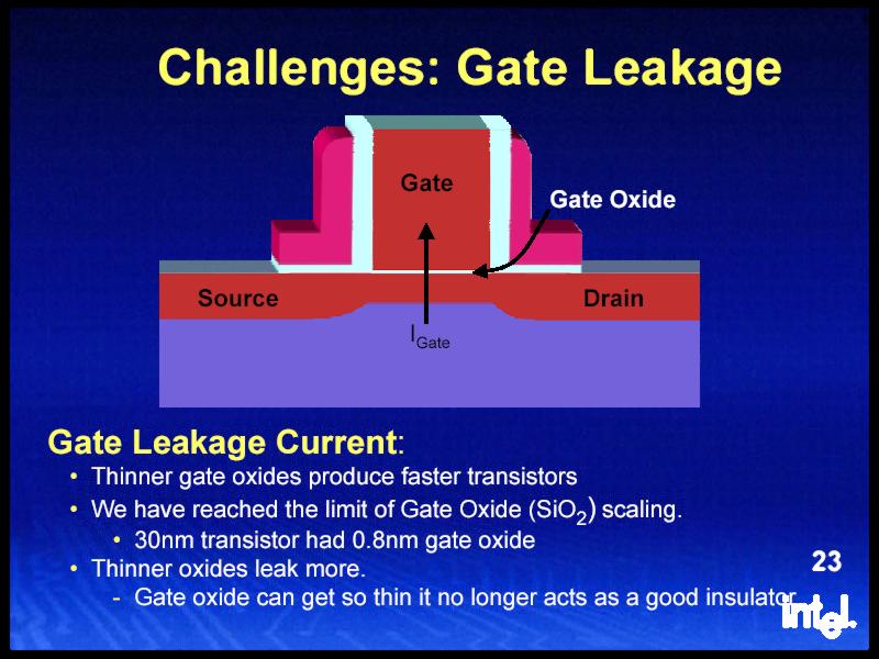
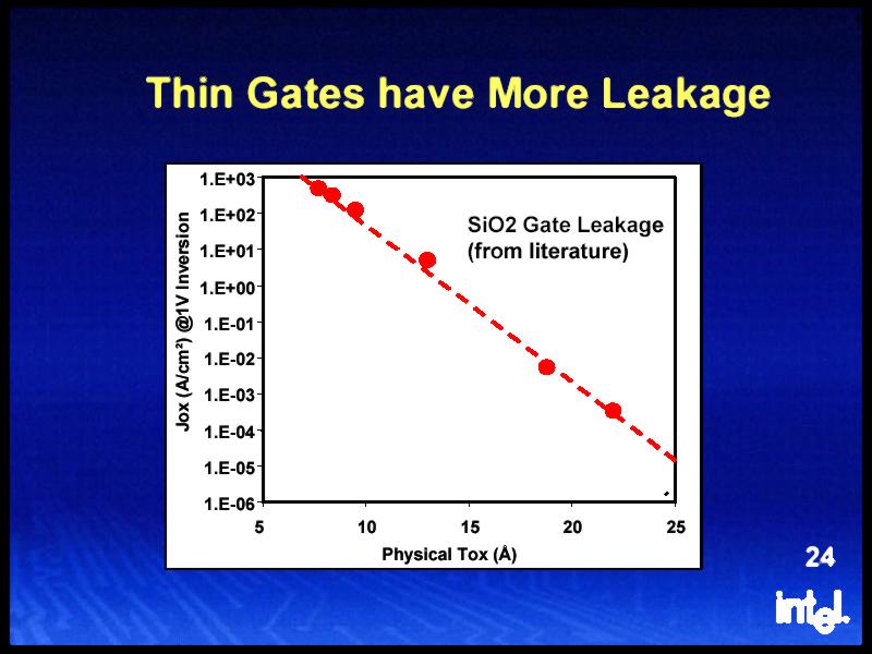
As we have already noted above in our analysis of the present 90nm and future 65nm process technology, silicon dioxide (SiO2) has been used as dielectric material for gates for 30 years already, mainly because its capacity to increase transistor performance by reducing the thickness of the insulating layer it forms. Nevertheless, further reduction of the oxide layer thickness (1.2 nm in 90nm and 65nm processes is only 5 atom layers!) is inevitably accompanied by undesirable effects. First of all, it's the increase of leakage current via the gate dielectric (IGate), which results in a considerable increase of power consumption and dissipation as well as "anomalous" transistor behaviour (note that these problems were the reason why the 90nm 4.0 GHz Pentium 4 Prescott processors had never come out and have been recently completely removed from the development program).
The problem of gate leakage current (IGate). On the left – explanation of the essence of the problem; on the right – dependence of leakage current on the gate oxide thickness.
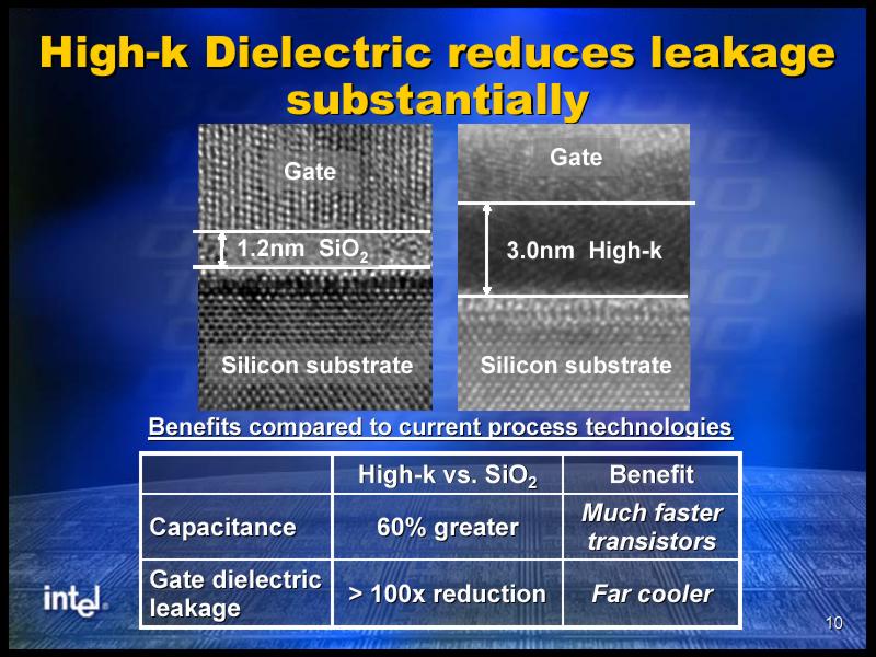
To solve this critical problem, Intel is planning to replace the current material of the gate dielectric (SiO2) with a thicker layer of the high-k material with better isolating properties, which creates high capacitance between the gate and the transistor channel (according to Intel, the "high-k" name derives from "high capacitance"). The first property of such material considerably reduces the leakage current, that is the "passive" power consumed by the transistor, while the second allows a considerably increased switching speed. Zirconium and hafnium oxides are noted in literature as preferable high-k materials.
High-k dielectrics as materials for a gate insulating layer.
Nevertheless, the use of high-k materials is presently significantly impeded by the problem of their "compatibility" with the electrode material – polycrystalline silicon (poly-Si). There appear two undesirable effects, when a high-k dielectric is combined with a polysilicon gate: Fermi level pinning and phonon scattering. The first effect is connected with some defects appearing on the border between the dielectric and the gate material and impeding the reduction of threshold voltage (i.e. the voltage level which switches the transistor state when applied to the gate), which is necessary to reach high transistor performance. The second effect is caused by the dielectric polarization, it reduces the mobility of charge carriers (electrons) and thus it also has a negative effect on the switching speed of transistors. To eliminate these undesirable effects, it's intended to use metallic gates (the choice of metal depends on the type of a transistor, PMOS or NMOS, and is currently not disclosed) and a special technique of transistor manufacturing. And finally, note that manufacturing such transistors as part of future Intel processors is expected in 2007 as an integral part of the 45nm process technology.
Lithographic tasks
Intel notes the following lithographic challenges of the future: the problem of feature size control and mask techniques. Before we proceed to the brief overview of these problems and their solutions, let's dwell on the lithographic process in general.
| Transistor dimensions |
Problems |
Solutions |
| 90-65 nm |
Size control |
Alternating Phase Shift Masks (APSM),
Optical Proximity Correction (OPC) |
| 65-30 nm |
Mask making |
EUV lithography (in far ultraviolet
spectrum) |
Lithography means the process of creating necessary structural units
of a chip. As a rule, the current chip generation is composed of a
silicon substrate with over 20 layers of various materials on its
surface, which form structural units – transistors and feature
connectors ("wires"), which combination specifies necessary
configuration of the final product – be it a microprocessor,
chipset, memory, or any other chip type.
The lithographic process actively employs so called "masks". They are like a black-and-white negative, but only two gradations are used instead of shades of gray – full light transmission and full light absorption. The masks themselves are composed of a glass substrate with a dye "pattern" on it. The pattern is transferred from the mask to a silicon plate by projecting light of a certain wavelength through the mask.
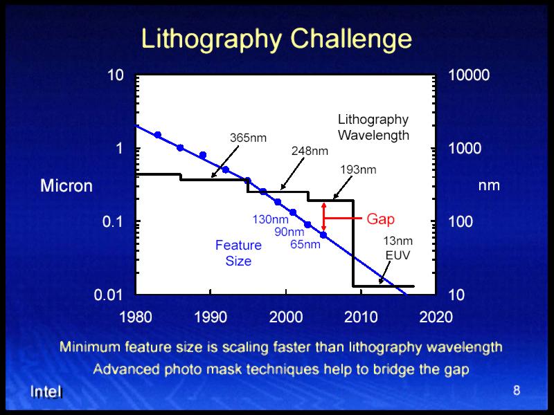
Lithography challenges for the nearest and distant future. The main problem is the increasing gap between the lithography wavelength and the decreasing feature size.
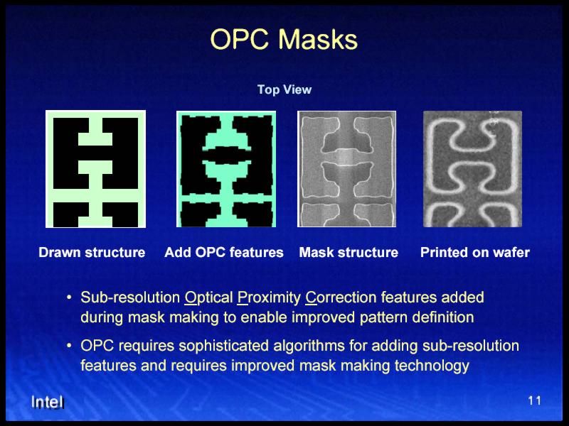
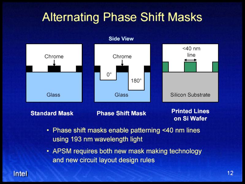
Development of the process technology as such obviously requires developing the lithography technique in use. The key element of the lithographic technique is the wavelength of the light source. Shorter-wave source allows smaller structural units, but this comes at the cost of the light source and optics as well as other system components. The present generation of Intel's chips is manufactured with an ultraviolet light source with the wavelength of 193nm, which allows minimum size of the structural unit of about 50nm (that is a gate length of a 90nm transistor). It's obvious that manufacturing 65nm transistors (with 35nm gate length, as was already mentioned above) requires either reduced wavelength of the light source or other tricks. These days Intel has taken up the second way by advancing alternative, more economically efficient technological tricks to increase pattern definition during the lithographic transfer of the mask pattern to the plate, which are called Alternating Phase-Shift Masks, APSM and Optical Proximity Correction, OPC. These technologies allow patterning substrates with the required minimum feature size, however they require significantly reworked mask making technology.
Lithographic solutions for the nearest future. Optical Proximity Correction and Alternating Phase-Shift Masks technologies in making and patterning masks.
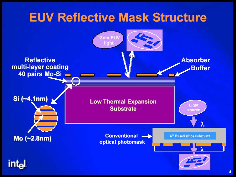
Nevertheless, the future process technologies will inevitably require a reduced wavelength of the emitter. Several presentations note the 157nm lithographic process as an intermediate solution. However, since the last IDF 2003 Russia, Intel has been planning the future lithographic techniques only as an introduction of the Extreme Ultra-Violet (EUV) technology with a huge wavelength leap of the light source far beyond the visible spectrum (which is within the 400-800nm wavelengths) into the far or hard ultra-violet radiation – to 13.5nm. While it's an obvious advantage from the point of view of resolution, a lot of technological problems are expected as well. The main problem is the absorption of such a short light by the lens material (quartz glass), which forces a fundamental technological reconstruction in the form of lens replacement with mirrors. In their turn, transmitting masks will have to be replaced with reflective ones (that is absorbing shortwave ultra-violet radiation in one spectrum and reflecting – in the other. Silicon molybdenum masks are planned to be used for this purpose). Besides, the entire plant must be put in absolute vacuum, because molecular nitrogen and oxygen also absorb well in this spectrum.
Lithographic techniques of the distant future. EUV lithography and reflective masks.
Conclusions
In fact, it's too early to make conclusions about the 65nm process technology, or moreover, about the future Intel technologies. As always, success or failure of the new technology will be demonstrated by ready solutions manufactured by this technology. And manufacturing 65nm processor cores is expected only next year. Besides, one can say that the process technology itself has not taken its final form yet. In our next articles we shall continue to review future semiconductor technologies, which are gradually becoming a part of the present. And there is nothing for us but to wait...
Write a comment below. No registration needed!