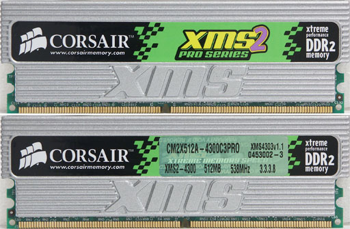
We proceed with the series of articles, dedicated to the low level analysis of the most important characteristics of DDR2 memory modules using our RightMark Memory Analyzer test package. In this article we are going to examine a pair of 512MB DDR2-533 modules of the XMS2 PRO series, manufactured by Corsair Memory. XMS2 PRO is a new series in the range of DDR2 XMS2 memory modules, manufactured by the company since mid 2003. It's high-performance DDR2 modules in stylish packaging notable for 24 activity indicators.
The layout of LEDs — activity indicators (2 x 12) can be seen on the photo below (side view). We didn't manage to figure out completely what exactly these LEDs indicate. We are inclined to think that they don't indicate the activities of individual logical banks of a module, but rather the general load of the memory bus in a given module — from the minimal level, indicated by the first four green LEDs, through the middle level (four yellow LEDs in the middle), up to the maximum level (the last four red LEDs).
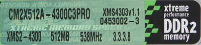
Module Part Number
The brief technical documentation on Corsair XMS2 PRO memory modules
(http://www.corsairmemory.com/corsair/products/specs/CM2X512-4300C3PRO.pdf)
provides no information on the expansion of some Part Number elements.
Nevertheless, the part numbering system of Corsair modules is rather
simple and is easy to decipher on one's own.
Field
Value
Expansion
0
CM
Manufacturer: CM = Corsair Memory
1
2X
Module type: 2X = DDR2
2
512
Module density: 512 MB
3
4300
Theoretical throughput of the module:
4300 MB/s
4
C3
CAS# Latency: 3
5
PRO
Module series: PRO
Out of additional technical characteristics of the modules, specified in the datasheet, we want to note the non-standard 538 MHz frequency, used by the manufacturer for testing the modules, and the recommended and written in SPD 3-3-3-8 timings, which are quite different from typical DDR2-533 timings (4-4-4-11 or 4-4-4-12).
SDRAM Cycle time (tCK) at maximum supported CAS# latency (CL X)
9
3Dh
3.75 ns (266.7 MHz)
DIMM configuration type
11
00h
Non-ECC
Refresh Rate/Type
12
82h
7.8125 ms — 0.5x reduced self-refresh
Primary SDRAM Width (organization type) of the memory module chips
13
08h
x8
Error Checking SDRAM Width (organization type) of the memory chips in the ECC module
14
00h
Not defined
Burst Lengths Supported (BL)
16
0Ch
BL = 4, 8
Number of Banks on SDRAM Device
17
04h
4
CAS Latency (CL)
18
08h
CL = 3
Minimum clock cycle (tCK) at reduced CAS# latency (CL X-1)
23
00h
Not defined
Minimum clock cycle (tCK) at reduced CAS# latency (CL X-2)
25
00h
Not defined
Minimum Row Precharge Time (tRP)
27
2Dh
11.25 ns (3, CL = 3)
Minimum Row Active to Row Active delay (tRRD)
28
1Eh
7.5 ns (2, CL = 3)
Minimum RAS to CAS delay (tRCD)
29
2Dh
11.25 ns (3, CL = 3)
Minimum Active to Precharge Time (tRAS)
30
1Eh
30.0 ns (8, CL = 3)
Module Bank Density
31
80h
512 MB
Write recovery time (tWR)
36
3Ch
15.0 ns (4, CL = 3)
Internal write to read command delay (tWTR)
37
1Eh
7.5 ns (2, CL = 3)
Internal read to precharge command delay (tRTP)
38
1Eh
7.5 ns (2, CL = 3)
SDRAM Device Minimum Active to Active/Auto Refresh Time (tRC)
41, 40
37h, 00h
55.0 ns (15, CL = 3)
SDRAM Device Minimum Auto-Refresh to Active/Auto-Refresh Command Period (tRFC)
42, 40
69h, 00h
105.0 ns (28, CL = 3)
Maximum device cycle time (tCKmax)
43
80h
8.0 ns
SPD Revision
62
10h
Revision 1.0
Checksum for Bytes 0-62
63
0Dh
13 (true)
Manufacturer’s JEDEC ID Code
64-71
7Fh, 7Fh, 9Eh
Corsair
Module Part Number
73-90
—
CM2X512A-4300C3PROMA
Module Manufacturing Date
93-94
00h, 00h
Not defined
Module Serial Number
95-98
00h, 00h, 00h, 00h
Not defined
According to the SPD data, the modules under review can operate only when the CAS# (CL X) latency is equal to three, with the 3.75ns clock cycle, i.e. 266.7 MHz (in DDR2-533 mode). A memory timing scheme for this case can be written as 3-3-3-8, which completely corresponds to the specifications. So, the low timing values expectedly result in a significant reduction of absolute tRP and tRCD values to 11.25 ns (typical value — 15 ns) and tRAS — to 30 ns (typical value — 40-45 ns). At the same time, in general other characteristics (tRC and especially tRFC) are almost no different from the typical DDR2-533 values.
Among the other features of the SPD chip is the lack of data on the manufacturing date and the module serial number, but the availability of information on the Part Number. For some reason, the "MA" lettering is added to the part number on the modules.
In the first series of tests we used the standard timing scheme, which was set in BIOS by default (Memory Timings: by SPD) on all our testbeds. As you can see from the table below, these motherboards have not agreed upon the "standards" and the reason is quite obvious — the timings written in SPD are too far from the typical DDR2-533 values. So, only one motherboard, Abit Fatal1ty AA8XE (Testbed #4), sets the manufacturer's default timings (3-3-3-8) correctly. Like all the other Gigabyte motherboards, Gigabyte 8AENXP-D tends to increment tCL by one resulting in the 4-3-3-8 timing scheme. We found it out before, when tested DDR memory modules "for overclockers". On the contrary, the motherboards from MSI and ECS set a faster scheme — 3-3-3-6. However, it makes absolutely no difference to the memory modules, because they are not an exception from the general "rule", discovered experimentally. According to this rule, tRAS values in chipset settings are ignored and internal values are used instead (in our case it's obviously 8).
Maximum Pseudo-Random Access Latency, ns
(without hardware prefetch)
95.4
99.6
96.6
95.1
—
87.5
89.9
Minimum Random Access Latency**,
ns
(without hardware prefetch)
108.9
119.6
111.2
109.2
—
100.2
104.1
Maximum Random Access Latency**,
ns
(without hardware prefetch)
128.7
139.8
131.0
128.3
—
119.4
122.3
*FSB frequency — 266.7 MHz
**16MB block size
With the FSB set to 200 MHz, the majority of motherboards on Intel 925X and 925XE (Testbeds #1, #3, and #4) demonstrate almost identical results. Strange as it may seem, the only exception is the ECS PF21 Extreme motherboard "for overclockers" (Testbed #2), which is noticeably outscored by the other models both in memory bandwidth (up to 200 MB/s) and in latency (up to 10 ns in random walks). Moreover, when switched to the 266MHz FSB mode, this very motherboard... refused to work with the modules under review at all. The other two models on i925XE (Testbeds #6 and #7) work fine in this mode, demonstrating a typical memory latency drop by approximately 10ns in all cases due to the synchronous mode (FSB:DRAM frequencies = 1:1).
Stability tests
Timing values (except for tCL, which cannot be reduced further!) were adjusted "on the fly" due to the built-in RMMA feature that allows to change dynamically memory settings supported by the chipset. Memory operation stability was evaluated in our specially developed utility, which will soon be released as a stand-alone application and will come shipped with RMMA.
While our motherboards disagree upon the "standard" timing values, the minimum values are selected unanimously. Nevertheless, the mere minimum timing values (allowed by these modules) are much more impressive than this fact, because they look absolutely fantastic for DDR2-533 — 3-2-2.
Maximum Pseudo-Random Access Latency, ns
(without hardware prefetch)
94.5
99.5
94.3
95.2
—
82.8
89.8
Minimum Random Access Latency**,
ns
(without hardware prefetch)
101.3
109.9
100.6
101.6
—
89.1
96.7
Maximum Random Access Latency**,
ns
(without hardware prefetch)
120.9
130.0
119.9
120.9
—
108.3
116.4
*FSB frequency — 266.7 MHz
**16MB block size
Overclocking the timings allows to improve the results, obtained on the ECS PF21 Extreme motherboard (Testbed #2), as well as to increase the maximum real memory read bandwidth to 8.2-8.4 GB/s (266 MHz FSB) and reduce the latencies approximately by 10 ns at random access.
Bottom line
Tested samples of Corsair DDR2-533 modules (XMS2 PRO series) provide
good compatibility with various motherboards on i925X and i925XE chipsets
in standard modes, they demonstrate good performance (memory bandwidth
and latencies are typical for high-performance modules operating in
DDR2-533 mode). We should also note the excellent overclocking potential
of these modules in terms of timings — the previous record (3-3-3),
cracked by Corsair XMS2
DDR2-667 (675) modules in DDR2-533 mode, is a nominal value for these
PRO modules. Their minimum timings, which still allow stable memory
operation (3-2-2), are an absolute record for DDR2-533 modules.
Corsair DDR2-533 XMS2 PRO modules have been provided
by the representative office of Corsair Memory in Russia