Updated: DDR Memory Analysis. Part 1: Micron DDR2 Modules
|
We call your attention to a new series of articles devoted to the analysis of the most important characteristics of memory modules on the low level. We shall use a universal test package RightMark Memory Analyzer, which we developed for this purpose. Its new version has been recently announced. Objective of this analysis is to provide our interested readers with information on compatibility of this memory module from this manufacturer with different mainboards based on various chipsets. By "compatibility" of the memory module with a mainboard we mean the balance between the maximum performance and stability of the module possible to achieve on this mainboard. It goes without saying that the higher is the performance of the memory module (i.e. greater real throughput and lesser latency) that we can get on a mainboard preserving operation stability in comparison with the other mainboards, other things being equal, the more reasonable is the choice of the given combo of the memory module and the mainboard.
By the way, in future we plan to provide this information automatically – it will be part of the functionality of our database (catalog) of memory modules, which is now in the development stage. The main function of this database will be to search for an optimal mainboard to a selected module (as it has been mentioned above, the search criterion is a balance of performance and stability) and vice versa. The database will grow with test results added by our developers as well as by users. Note that the option to submit test results was implemented in Version 3.2 of our test package RightMark Memory Analyzer.
Thus the present article can be considered sort of an information model, which should be presented to users by their requests from our database. In this connection, we are looking forward to any feedback from our readers on how we should present this information to make it most comfortable to perceive and use. And now we proceed to the analysis of our today's memory module sample.
Manufacturer Information
Module manufacturer: Micron Technology, Inc.
Chip manufacturer: Micron Technology, Inc.
Web site of the module manufacturer: http://www.micron.com/products/modules/ddr2sdram/
Web site of the chip manufacturer: http://www.micron.com/products/dram/ddr2sdram/
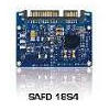
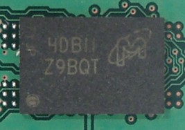
Module Appearance
Photo of the memory module
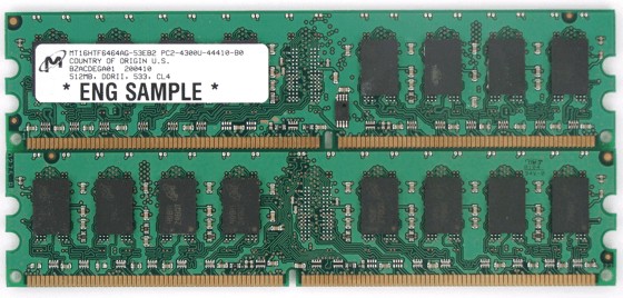
Photo of the memory chip
Part Numbering System of Modules and Chips
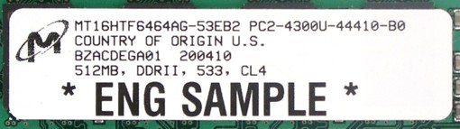
Module Part Number Expansion
Part numbering system of Micron memory modules and chips:
http://www.micron.com/numberguide/
| Field |
Value |
Expansion |
| 0 |
MT |
Manufacturer code:
MT = Micron Technology |
| 1 |
16 |
Number of memory chips |
| 2 |
H |
Protocol:
H = SSTL 1.8V DDR2 SDRAM |
| 3 |
TF |
Product family:
TF = DDR2 FBGA |
| 4 |
64 |
Module depth, bit |
| 5 |
64 |
Module width, bit |
| 6 |
A |
Module version:
A = 168-pin/184-pin/240-pin unbuffered DIMM |
| 7 |
G |
Package code:
G = lead plating, one- or two-bank DIMM |
| 8 |
-53E |
Speed characteristics of the module:
-53E = DDR2-533, PC2-4300, timings 4-4-4 |
| 9 |
B |
Chip revision number |
| 10 |
2 |
PCB revision number |
Chip Part Number Expansion
| FBGA code |
Part Number |
| Z9BQT |
MT47H32M8FP-37E ES |
Due to space limitations, FBGA-packaged Micron memory chips have an abbreviated part marking that is different from the part number. Thus, chip marking of the Z9BQT memory module is decoded into the following part number: MT47H32M8FP-37E ES. You can decode an abbreviated part marking of any Micron memory chip into a part number at http://www.micron.com/decoder/
| Field |
Value |
Expansion |
| 0 |
MT |
Manufacturer code:
MT = Micron Technology |
| 1 |
47 |
Product family:
47 = DDR2 |
| 2 |
H |
Process technology:
H = SSTL 1.8V VDD CMOS |
| 3 |
32M8 |
Device type: 256Mbit (32Mbit x8) |
| 4 |
|
Device version (n/a) |
| 5 |
FP |
Package code:
FP = lead plating, FBGA, 60-pin 8x12 |
| 6 |
-37E |
Access/cycle time:
-37E = 3.75 ns (266.7 MHz), 4-4-4 |
| 7 |
|
Operating temperatures:
Blank = 0..85oC |
| 8 |
|
Special options (n/a) |
| 9 |
ES |
Special processing:
ES = engineering sample |
SPD module chip data
Description of the SPD general standard:
JEDEC Standard No. 21-C, 4.1.2 - SERIAL PRESENCE DETECT STANDARD, General Standard
Description of the SPD specific standard for DDR2:
JEDEC Standard No. 21-C, 4.1.2.10 - Appendix X: Specific SPDs for DDR2 SDRAM (Revision 1.0)
JC-45 Appendix X: Specific PD's for DDR2 SDRAM (Revision 1.1)
| Function |
Byte |
Value |
Expansion |
| Fundamental Memory Type |
2 |
08h |
DDR2 SDRAM |
| Number of Row Addresses on this assembly |
3 |
0Dh |
13 (RA0-RA12) |
| Number of Column Addresses on this assembly |
4 |
0Ah |
10 (CA0-CA9) |
| Number of DIMM Banks |
5 |
61h |
2 physical banks |
| Data Width of this assembly |
6 |
0x40 |
64 bit |
| Voltage Interface Level of this assembly |
8 |
0x05 |
SSTL 1.8V |
| SDRAM Cycle time (tCK) at maximum supported CAS# latency (CL X) |
9 |
3Dh |
3.75 ns (266.7 MHz) |
| DIMM configuration type |
11 |
00h |
Non-ECC |
| Refresh Rate/Type |
12 |
82h |
7.8125 ms – 0.5x reduced self-refresh |
| Primary SDRAM Width (organization type of the memory module chips) |
13 |
08h |
x8 |
| Primary SDRAM Width (organization type of the memory module chips) of the ECC module |
14 |
00h |
Not defined |
| Burst Lengths Supported (BL) |
16 |
0Ch |
BL = 4, 8 |
| Number of Banks on SDRAM Device |
17 |
04h |
4 |
| CAS Latency (CL) |
18 |
18h |
CL = 3, 4 |
| Minimum clock cycle (tCK) at reduced CAS latency (CL X-1) |
23 |
50h |
5.00 ns (200.0 MHz) |
| Minimum clock cycle (tCK) at reduced CAS latency (CL X-2) |
25 |
00h |
Not defined |
| Minimum Row Precharge Time (tRP) |
27 |
3Ch |
15.0 ns
4, CL = 4
3, CL = 3 |
| Minimum Row Active to Row Active delay (tRRD) |
28 |
1Eh |
7.5 ns
2, CL = 4
1.5, CL = 3 |
| Minimum RAS to CAS delay (tRCD) |
29 |
3Ch |
15.0 ns
4, CL = 4
3, CL = 3 |
| Minimum Active to Precharge Time (tRAS) |
30 |
2Dh |
45.0 ns
12, CL = 4
9, CL = 3 |
| Module Bank Density |
31 |
40h |
256 MB |
| Write recovery time (tWR) |
36 |
3Ch |
15.0 ns
4, CL = 4
3, CL = 3 |
| Internal write to read command delay (tWTR) |
37 |
1Eh |
7.5 ns
2, CL = 4
1.5, CL = 3 |
| Internal read to precharge command delay (tRTP) |
38 |
1Eh |
7.5 ns
2, CL = 4
1.5, CL = 3 |
| Minimum Active to Active/Refresh Time (tRC) |
41, 40 |
3Ch, 00h |
60.0 ns
16, CL = 4
12, CL = 3 |
| Minimum Refresh to Active/Refresh Command Period (tRFC) |
42, 40 |
4Bh, 00h |
75.0 ns
20, CL = 4
15, CL = 3 |
| Maximum device cycle time (tCKmax) |
43 |
80h |
8.0 ns |
| SPD Revision |
62 |
10h |
Revision 1.0 |
| Checksum for Bytes 0-62 |
63 |
11h |
17 (true) |
| Manufacturer’s JEDEC ID Code |
64-71 |
2Ch, FFh,
..., FFh |
Micron |
| Module Part Number |
73-90 |
|
16HTF6464AG-53EB2 |
| Module Manufacturing Date |
93-94 |
04h, 0Bh |
year 2004, week 11 |
| Module Serial Number |
95-98 |
10h, 23h,
19h, 1Ch |
1C192310h |
Analysis of the SPD chip data shows that this module supports CAS latencies (CL) of 4 and 3 cycles. The former corresponds to the timing loop of 3.75 ns, so it is recommended to be used at 266 MHz, that is in DDR2-533 mode. The latter – 5.00 ns timing loop, that is it's recommended to be used at 200 MHz in DDR2-400 mode. The corresponding timings (tCL- tRCD-tRP-tRAS) can be recorded as 4-4-4-12 for the native DDR2-533 mode and 3-3-3-9 for DDR2-400 mode.
It's interesting to note that tRAS values (Minimum Active to Precharge Time) marked on the module (10 cycles) and on its SPD chip (12 cycles) do not match. Let's hope that this inconsistency is peculiar only to the engineering sample under review in our lab. Anyway, for our tests we set the timings in BIOS to 4-4-4-11, and thus tRAS was set in between the two settings "recommended" by the manufacturer.
Testbed Configurations and Software
Mainboards based on the chipsets of Intel i915 series
Testbed #1
- CPU: Intel Pentium 4 3.6 GHz (Prescott core, 1 MB L2)
- Chipset: Intel i915P
- Mainboard: Gigabyte 8GPNXP Duo, BIOS v.F2
- Memory: 2x512 MB Micron DDR2-533, 4-4-4-11 timings
- Video: Leadtek PX350 TDH, nVidia PCX5900
- HDD: WD Raptor WD360, SATA, 10000 rpm, 36Gb
- Drivers: nVidia Forceware 62.01, Intel Chipset Utility 6.0.1.1002, DirectX 9.0b
Testbed #2
- CPU: Intel Pentium 4 3.6 GHz (Prescott core, 1 MB L2)
- Chipset: Intel i915G
- Mainboard: Foxconn 915M03-G-8EKRS2, BIOS v.5/29/2004
- Memory: 2x512 MB Micron DDR2-533, 4-4-4-11 timings
- Video: Leadtek PX350 TDH, nVidia PCX5900
- HDD: WD Raptor WD360, SATA, 10000 rpm, 36Gb
- Drivers: nVidia Forceware 62.01, Intel Chipset Utility 6.0.1.1002, DirectX 9.0b
Testbed #3
- CPU: Intel Pentium 4 3.6 GHz (Prescott core, 1 MB L2)
- Chipset: Intel i915G
- Mainboard: Foxconn 915M03-G-8EKRS2, BIOS v.5/29/2004
- Memory: 2x512 MB Micron DDR2-533, 4-4-4-11 timings
- Video: Internal, 32 MB
- HDD: WD Raptor WD360, SATA, 10000 rpm, 36Gb
- Drivers: Intel VGA 14.5, Intel Chipset Utility 6.0.1.1002, DirectX 9.0b
Testbed #4
- CPU: Intel Pentium 4 3.6 GHz (Prescott core, 1 MB L2)
- Chipset: Intel i915G
- Mainboard: Intel D915GUX, BIOS v.0234
- Memory: 2x512 MB Micron DDR2-533, 4-4-4-11 timings
- Video: Leadtek PX350 TDH, nVidia PCX5900
- HDD: WD Raptor WD360, SATA, 10000 rpm, 36Gb
- Drivers: nVidia Forceware 62.01, Intel Chipset Utility 6.0.1.1002, DirectX 9.0b
Testbed #5
- CPU: Intel Pentium 4 3.6 GHz (Prescott core, 1 MB L2)
- Chipset: Intel i915G
- Mainboard: Intel D915GUX, BIOS v.0234
- Memory: 2x512 MB Micron DDR2-533, 4-4-4-11 timings
- Video: Internal, 32 MB
- HDD: WD Raptor WD360, SATA, 10000 rpm, 36Gb
- Drivers: Intel VGA 14.5, Intel Chipset Utility 6.0.1.1002, DirectX 9.0b
Testbed #6
- CPU: Intel Pentium 4 3.6 GHz (Prescott core, 1 MB L2)
- Chipset: Intel i915P
- Mainboard: ASUS P5GD2 Premium, BIOS v.1004
- Memory: 2x512 MB Micron DDR2-533, 4-4-4-11 timings
- Video: Leadtek PX350 TDH, nVidia PCX5900
- HDD: WD Raptor WD360, SATA, 10000 rpm, 36Gb
- Drivers: nVidia Forceware 62.01, Intel Chipset Utility 6.0.1.1002, DirectX 9.0b
Mainboards based on the chipsets of Intel i925 series
Testbed #7
- CPU: Intel Pentium 4 3.6 GHz (Prescott core, 1 MB L2)
- Chipset: Intel i925X
- Mainboard: Gigabyte 8ANXP-D, BIOS v.F2
- Memory: 2x512 MB Micron DDR2-533, 4-4-4-11 timings
- Video: Leadtek PX350 TDH, nVidia PCX5900
- HDD: WD Raptor WD360, SATA, 10000 rpm, 36Gb
- Drivers: nVidia Forceware 62.01, Intel Chipset Utility 6.0.1.1002, DirectX 9.0b
Testbed #8
- CPU: Intel Pentium 4 3.6 GHz (Prescott core, 1 MB L2)
- Chipset: Intel i925X
- Mainboard: Intel D925XCV, BIOS v.0218
- Memory: 2x512 MB Micron DDR2-533, 4-4-4-11 timings
- Video: Leadtek PX350 TDH, nVidia PCX5900
- HDD: WD Raptor WD360, SATA, 10000 rpm, 36Gb
- Drivers: nVidia Forceware 62.01, Intel Chipset Utility 6.0.1.1002, DirectX 9.0b
Testbed #9
- CPU: Intel Pentium 4 3.6 GHz (Prescott core, 1 MB L2)
- Chipset: Intel i925X
- Mainboard: ASUS P5AD2 Premium, BIOS v.1004
- Memory: 2x512 MB Micron DDR2-533, 4-4-4-11 timings
- Video: Leadtek PX350 TDH, nVidia PCX5900
- HDD: WD Raptor WD360, SATA, 10000 rpm, 36Gb
- Drivers: nVidia Forceware 62.01, Intel Chipset Utility 6.0.1.1002, DirectX 9.0b
Test Results
Mainboards based on the chipsets of Intel i915 series
| Parameter* |
Testbed 1 |
Testbed 2 |
Testbed 3 |
Testbed 4 |
Testbed 5 |
Testbed 6 |
Testbed 6 (PAT) |
| Average memory read bandwidth, MB/sec |
4782 |
4736 |
4558 |
4729 |
4548 |
4755 |
5185 |
| Average memory write bandwidth, MB/sec |
2024 |
2205 |
2204 |
2212 |
2200 |
2219 |
2246 |
| Max. memory read bandwidth, MB/sec |
6383 |
6388 |
6073 |
6345 |
6067 |
6425 |
6488 |
| Max. memory write bandwidth, MB/sec |
4266 |
4245 |
4245 |
4238 |
4238 |
4260 |
4293 |
| Minimum Pseudo-Random Access Latency, ns** |
50.4 |
50.9 |
52.3 |
50.9 |
52.3 |
50.6 |
46.4 |
| Maximum Pseudo-Random Access Latency, ns** |
57.2 |
57.8 |
59.0 |
57.9 |
59.1 |
57.5 |
52.9 |
| Minimum Random Access Latency, ns** |
120.3 |
121.0 |
123.0 |
121.3 |
123.1 |
120.5 |
105.4 |
| Maximum Random Access Latency, ns** |
138.6 |
139.4 |
141.0 |
139.7 |
141.3 |
139.0 |
124.0 |
*the best results are in bold
**Block size – 16 MB
As we have already mentioned in the previous analysis, the current generation of processors and chipsets with the FSB frequency of 800 MHz does not allow to reach the maximum DDR2-533 throughput in dual channel mode. Nevertheless, even in this case we can draw certain conclusions about the real memory bandwidth, which can be achieved on various mainboards.
Among the mainboards based on the Intel i915 series chipsets the obvious leader absolutely by all parameters is ASUS P5GD2 Premium (Testbed #6) in PAT mode (Turbo mode). This advantage comes into particular prominence in the average memory read bandwidth (5185 MB/sec) and in Random Access Latency (105.4 ns). Nevertheless, the same mainboard with PAT disabled already loses to Gigabyte 8GPNXP Duo (Testbed #1) equipped with the same i915P chipset, which occupies the second place by the majority of parameters (except for a strange Average memory write bandwidth of 2024 MB/sec instead of the typical 2200 MB/sec). And the worst results are demonstrated by the mainboards on i915G – both Foxconn 915M03-G-8EKRS2 (Testbeds #2, 3) and Intel 915GUX (Testbeds #4, 5), especially with the enabled on-board video controller (which reduces the maximum real memory bandwidth and raises the memory latency approximately by 4%). Note how close the module characteristics taken from both mainboards are with integrated video enabled and disabled.
Mainboards based on the chipsets of Intel i925 series
| Parameter* |
Testbed 7 |
Testbed 8 |
Testbed 9 |
Testbed 9 (PAT) |
| Average memory read bandwidth, MB/sec |
4949 |
4906 |
4934 |
5366 |
| Average memory write bandwidth, MB/sec |
2261 |
2256 |
2331 |
2388 |
| Max. memory read bandwidth, MB/sec |
6458 |
6401 |
6399 |
6494 |
| Max. memory write bandwidth, MB/sec |
4266 |
4238 |
4260 |
4293 |
Minimum Pseudo-Random
Access Latency, ns** |
47.7 |
48.1 |
47.8 |
43.6 |
Maximum Pseudo-Random
Access Latency, ns** |
54.6 |
55.0 |
54.7 |
50.3 |
Minimum Random
Access Latency, ns** |
115.2 |
116.2 |
115.6 |
100.6 |
Maximum Random
Access Latency, ns** |
133.6 |
134.7 |
134.0 |
119.7 |
*the best results are in bold
**Block size – 16 MB
First of all it should be noted that on the whole mainboards on i925X outscore mainboards based on i915P/G by all parameters. The leader here is again the mainboard from ASUS (P5AD2 Premium, Testbed #9), but again only with PAT mode enabled (Turbo mode). When this mode is disabled, the mainboard goes down to the third place giving the pas to Gigabyte 8ANXP-D (Testbed #7). The worst choice among the mainboards on i925X is Intel D925XCV (Testbed #8).
Results
Thus, from the point of view of the maximum performance of DDR2 Micron modules (other things being equal) the best mainboards are the ones from ASUS based on Intel i925X and i915P chipsets. Mainboards from Gigabyte (8ANXP-D and 8GPNXP Duo) based on the same chipsets are losing to the leader, but not much. And the worst option in respect to maximum performance of the memory subsystem are the mainboards Intel 915GUX and Foxconn 915M03-G-8EKRS2 based on Intel i915G (which demonstrated almost the same results), especially with the integrated video controller enabled.
Write a comment below. No registration needed!
|
|
 |
|
|
|