 |
||
|
||
| ||
|
||
|
||
| ||
1. What is volt modification?It's not easy to answer the question whether volt-modification is needed to survive when gaming requirements for hardware, in particular video adapters, are getting tougher, or it is a way to squeeze more potential from a video card to get more FPS in games. The video card tested today has a performance level sufficient for all existent games, that is why it matches the latter option. For low-level solutions such modification is a way to get more FPS needed for acceptable gameplay. Volt-modification is an attempt to increase a video card's overclocking potential by changing its internal working voltages (memory, GPU, I/O circuits). But such attempt doesn't guarantee a higher performance. This procedure is identical to changing CPU and memory voltages from BIOS. One can resort to it if a given video card doesn't provide such software means. 2. What is it for?For this video card volt-modification simply demonstrates its overclocking potential because its performance in gaming applications is not critical. Reasons for volt-modification:
I must say that we didn't aim at overclocking the video card extremely for revealing core and memory maximum potential (with various coolants) but wanted to get the fastest possible system that would match any home PC. 3. Materials and toolsThe list below shows the tools we used, but it is not a reference set. Any component can be replaced at your option. Materials and tools (commented):
You will also need documentation and circuit diagrams (see the details below). Before starting volt-modification you have to carry out effective... 4. Preliminary testingWell, it's time to have a look at the video card's specs. In this section
we test the pre-overclocking performance. The scores will be further used
for estimating the performance increase after overclocking.
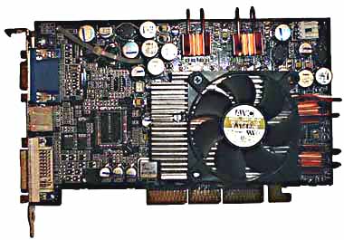
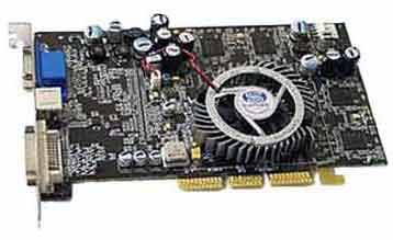 Fig. 1. Sapphire RADEON 9700 vide card with reference PCB design
Testbed:
Test applications:
We didn't make a special accent on testing the card's performance because the today's aim is to find out if volt-modification is justified. The test conditions are ordinary: running applications (Apache, Ftp server, VirtualCD, PowerStrip, LanChat, CdSlow) were not taken out of memory. Note: Test modes for Quake 3 Arena:
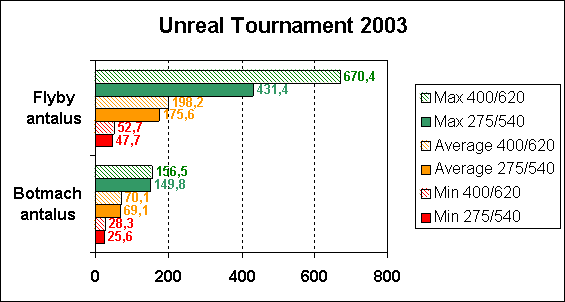
Test modes for Unreal Tournament 2003:
Test modes for 3DMark 2003 v.340 and 3DMark 2001 SE v.330: default settings Scores for 275/540:
 Fig. 2. 3DMark 2003 at 275/540
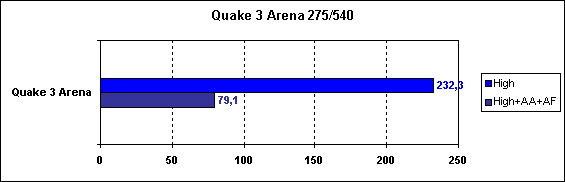 Fig. 3. Quake3 Arena at 275/540
 Fig. 4. Unreal Tournament 2003 at 275/540
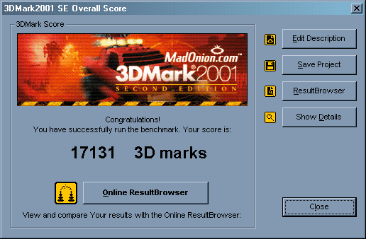
 Fig. 5. 3DMark 2001 SE
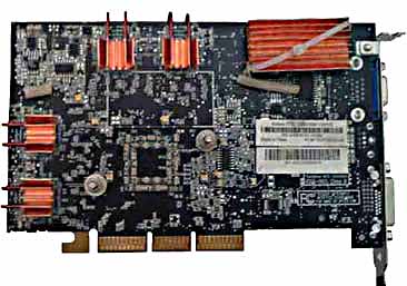
5. CoolingThe GPU has the following cooler:  Fig. 6. Standard coolerThis compact cooler is able to ensure a reliable operation of the GPU at the default clock speeds as air is taken out in all planes. But the cooler is not big enough for overclocking. Besides, the fan is pretty small and its fast rotation makes a lot of noise. Moreover, this particular fan turned out to be of low quality, and 2 months after its purchase it outcried all other fans and produced sounds unpleasant for human ears. The video memory had no cooler at all. Taking into account the layout of all the components let's design a new cooler. 5.1. MaterialsThe new heatsink is based on Thermaltake's Vulcano 6 Cu because it has the matching size, a big copper plate in the base to ensure better heat removal; besides, it's not that expensive. 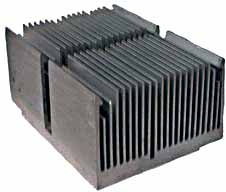 Fig. 7. GPU heatsinkThe heatsink (without a fan)) measures 80*40*62 mm. The copper cooler marked AVC C6010B12H was used for the memory. Since we plan on overclocking the memory up to the upper limit, such solution will considerably increase heat removal. That is why we needed an effective passive (for quiet operation) cooler, and we have decided on that inexpensive copper heat sink. 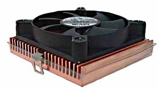 Fig. 8. Heatsink for video memory5.2. Designing, assembling and mountingNow we turn to designing a cooler. Before installation of the heatsink we made it twice lower - 20 mm. It's sufficient for effective cooler, and such design won't lock free PCI slots on mainboards which have the first PCI slot facing up (EPOX 8RDA3+). Such boards have a 35mm gap between the AGP and first PCI slots. We made holes in the sink base for projecting parts. Their size and location were experimentally calculated due to the difference in PCB designs, rated values (and sizes) of the parts and their location. When we installed the sink for the first time it turned out that the metallic frame that protected the GPU seated unevenly. The sink couldn't tightly abut on the chip, and the latter quickly overheated. We didn't remove the frame as it could damage the GPU, but we made a cut (0.5 mm) in the sink base: 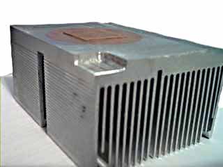 Fig. 9. Heatsink for GPU after millingThe mount was polished and the heatsink was tightly pressed against the GPU. After that the card worked steadily. The sink was outfitted with a fan from the AVC cooler (the fan was of very high quality): 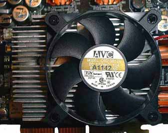 Fig. 10. Cooler mounted on the video cardATTENTION! The fan is shifted from the die center as far as the heatsink size makes it possible. It was done to prevent the dead area (area under the fan center without any air flows) above the die and make the latter blown with a strong air flow (which increases as the distance from the fan's center grows up). The sink is screwed through the standard holes in the video card. Let's dwell on the procedure of pressing and clamping the sink to the card. The screw-bolt has the following parts on underneath:
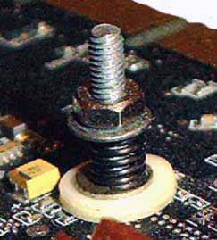 Fig. 11. GPU heatsink mounting
After that we made 8 small heatsinks out of the AVC sink (sawed it into 8 ones), each being a bit larger than the memory chip. The remaining part of the sink used for cooling the GPU voltage regulator. The only problem in installation of the heatsinks was their mounting. We didn't want to glue the chips because we could have problems when removing the heat sinks, and decided to fix them with clips. The principle of their operation is based on the metal memory effect: after putting it into a certain shape by bending and unbending it within certain limits the metallic part tends to return to the original state (before unbending). We used a copper wire 2 mm in diameter as a clip; its ends press down the heatsinks mounted onto the memory on both sides. Have a look at the result: 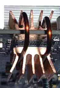
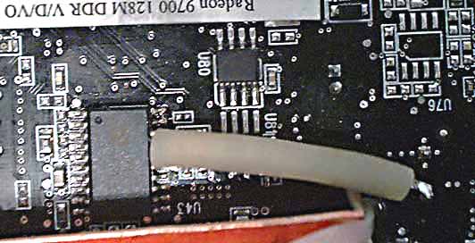
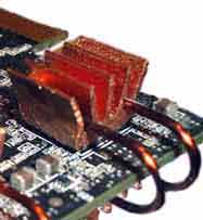 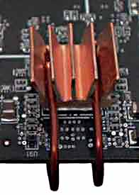 Fig. 12-14. Video memory coolerNow it's necessary to provide effective cooling of the GPU voltage changer chips (because overclocking causes higher power supply, which makes the stabilizing chips warmer). For that purpose you must remove the heat distributing aluminum plate. ATTENTION! Remove it very carefully as it's attached to the chips with thermal glue. It's very simple to damage the chips - in our case one of them remained on the heatsink and the video card stopped working. Besides, it's almost impossible to find a substitute. We were lucky to find a similar chip from the damaged GF3Ti200 128 MB card (ABIT Siluro). After that the copper sink the mount of which was modified so that it didn't get in the radio elements' road was installed onto the voltage changer. The clamp fixed the system. Here it is: 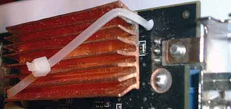 Fig. 15. Cooler for the voltage changer6. Volt-modification6.1. PreparationFor volt-modification we need a soldering iron, a digital multimeter with the internal resistance at least 10 MOhm (it's needed to exclude the measurement error of the multimeter). In our case it was MASTECH MY-65. Wire (you'd better use a braid of three wires as it makes the connection to the control points more reliable and easily accessible), two precise variable resistors (they should be wire-wound resistors because of small Ohm steps), and their accuracy should be within 1-10%. Rated values: 30 to 100 KOhm. ATTENTION! The theoretical maximum memory clock speed can be calculated by dividing 1000 by the memory access time in nanoseconds. In our case the access time was 3.3 ns, that is why the maximum possible working frequency was 303 MHz, or 606 MHz taking into account the DDR type. Before increasing the memory power supply the clock rate was 570 MHz, i.e. much lower than the limit. Memory voltage is usually lowered by manufacturers to separate the market segments. The fact that the memory clock speeds exceeded the theoretical ones after the volt modification procedure was to the credit of the given sample. That is why if it's possible to overclock memory on your card using the software means think well before starting volt modification (the experience show that the working clock speeds almost always exceed theoretical ones after such modification). 6.2. Memory volt-modificationIn our case the memory volt-modification was carried out because the memory
didn't properly overclock at the rated power supply which MUST be
measured before the process is started. For that purpose we took the
documentation from the manufacturer - in our case it's ISL6522 memory
internal circuits power supply pulse-width modulation controller (fig.
16) from For the measurements you have to solder the wires to the outputs 8 (+ internal circuits (VDD) of the memory chips), 7 (GND common) and 5 (a padding resistor (which should be variable at the first state of resistance selection) is soldered between the 5 and 7 outputs). Voltage is measured between outputs 7 and 8, and it was 2.8V in our case. We DO NOT RECOMMEND that you take our values as reference ones because you will most probably have different ones as it depends on the card maker and its memory. Even the same cards from different lots can differ. The output voltage of the internal memory power supply circuits is assigned by the resistance ratio in the feedback circuit. To increase the power supply voltage you should change this ratio by adding a padding resistor; it makes the voltage on the feedback circuit output lower, and the controller which compares it to the reference one increases this voltage up to the needed level, though the real voltage turns out to be increased.  Fig. 16. Reference diagram of pulse-width modulation controller ISL6522 (the padding resistor added is red)The 47 kOhm wire-wound resistor of 10% tolerance was chosen as a variable one. ATTENTION! While increasing the core and memory voltage we recommend that you solder a fixed resistor of 1.5 to 2 kOhm in parallel to the variable one. Without the additional resistor the variable resistance can drop much causing an increase in power supply on the respective blocks. These measures avoid damage of the card. Now we proceed to the key operation - the voltage increase. Measurements and parameters setting should be carried out very carefully and accurately as these circuits are very sensitive to any kinds of pickups, and even if you slightly touch the bared wire, the video card can hang making you restart the computer (the reset button won't help). The voltage must be controlled with a multimeter. You should lift it up in small steps reducing the variable resistance and controllong the variable resistor every time if you don't have an additional resistor in parallel to the variable one. The maximum voltage which can be reached in most cases is 3.2- 3.3V. However, you can try to get more at your own risk. At the higher voltage it can be insufficient to have only the passive cooler. For our video card the end-point output voltage of the internal memory power supply stages was 3.28V, which is a reasonable compromise of the danger of having the card damaged and its overclocking. After the voltage is lifted up you should carry out some tests with the memory clock increased, and if everything it okay, you must unsolder the resistor, measure the resultant resistance and replace it with an identical additional resistor (if you can't get it with one resistor, you can use a parallel of series connection of 2 or more resistors). The resistors should be covered with protective cambric. Here is how it looks like after all the operations:  Fig. 17. Modified memory power supply chip6.3. GPU volt modificationTo increase the GPU stability at the increased clock speeds and to prevent any artifacts in case of overclocking at the rated power supply (we could see a chessboard-like screen and a distorted shape of some 3D objects in some screen parts) you should raise the GPU power supply. In contrast to the memory volt-modification, for the GPU you increase the voltage on a different power supply controller chip. The padding resistance and location of the control points change at that. The safety margin of the voltage changing is 10 - 30% relative the
default value. The standard supply voltage makes 1.5V in many cases.
This voltage is controlled by the double synchronous low-power direct-voltage
controller with the combined current circuits SC1175 from The chip has two independent voltage control and stabilization channels, but in this case they are connected in parallel: 
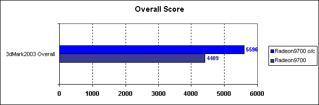
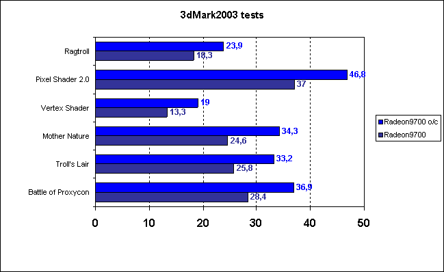
The overall performance increase in 3DMark 2003 is 27%. Performance gain in subtests:
The overall performance increase in Quake 3 Arena:
The overall performance increase in Unreal Tournament 2003:
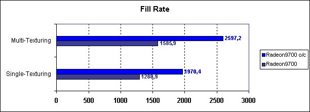
The overall performance increase in 3DMark 2001 SE is 18.6%. Performance gain wasn't estimated in the separate subtests of 3DMark 2001 SE. The general performance increase is 25-30% in all applications. Judging by the 3DMark 2003 the picture looks logical: the heavier the test, the greater the speed drop because of the great load on the video card. The texturing speed is 1.5 times greater at least, and it will have a positive effect on games that deal with large textures. In Quake 3 Arena in the heavy mode the overclocking has a greater effect too as the load is greater. In Unreal Tournament 2003 the scores depend mostly on the CPU. Now, when the card has a nice appearance, let's also modify its BIOS. 7. BIOS modificationThere are several reasons why we decided to change the BIOS parameters:
7.1. Possible problemsThere can be several problems:
7.2. ResultsAfter all those time-taking experiments with the BIOS we got only one important advantage: new clock speeds were flashed into the BIOS. At the same time we changed the TV standard from NTSC to PAL. All the experiments gave us more food for thought. Software used for video card overclocking and BIOS modification:
8. ConclusionWe spent quite a lot of time for all the designing and developing and got a card the performance of which increased by 25-30%. The Sapphire RADEON 9700 performs even better than the PRO version. This card can be named Sapphire RADEON 9700 XT. We described all the problems we faced when improving the adapter. And we hope that this article will help those who'd want to carry out volt modification of their cards. We believe that this review will help you decide whether it's worth modifying your card this way. NOTE! Do not do it if:
Surprise!This volt modification process was recorded! The clip can be downloaded
from here (95 MBytes!). We
express our gratitude to Driver.Ru and Sergei Komarov.
Artem Sokolovsky (voltmod@tut.by)
Pavel Shilenok (voltmod@tut.by)
Write a comment below. No registration needed!
|
Platform · Video · Multimedia · Mobile · Other || About us & Privacy policy · Twitter · Facebook Copyright © Byrds Research & Publishing, Ltd., 1997–2011. All rights reserved. |