 |
||
|
||
| ||
|
||
|
||
| ||
Before this test packet was created there was no proper software for measuring system's vital parameters such as CPU/Chipset/RAM providing steady and reliable (reproducible) test results and allowing for changing test parameters in a wide range. Among vital low-level system characteristics are latency and real RAM bandwidth, average/minimal latency of different cache levels and its associative level, a real L1-L2 cache bandwidth and TLB levels specs. Besides, these aspects are not paid sufficient attention to in a product's technical documentation (CPU or chipset). Such test packet which combines a good deal of subsets aimed at measuring objective system characteristics is much needed for estimating crucial objective platform's parameters. The test packet is developed within RightMark, named RightMark Memory Analyzer and available as an open source code. System requirementsMinimal system requirements:
 General settingsThis sector contains general settings of all subtests realized in RMMA. CPU Clock, CPU CountData on CPU clock and the number of logic processors in the system. Cache Line SizeThe effective cache line size detected automatically when a given application starts (detection takes only several seconds). This parameter is very important in achieving correct results in most realized subtests. That is why its automatic detection is an integral part of RMMA. Memory AllocationChoice of a method of allocation of memory needed for execution of the tests. Standard - standard method of memory block allocation with malloc() with the further usage of VirtualLock() on the memory region selected which guarantees that later accesses to this region won't cause page fault. AWE - this method uses Address Windowing Extensions available in Windows 2000/XP/2003 Server. This memory allocation method is more reliable for some tests such as cache associativity. Usage of AWE requires Lock Pages in Memory privilege which is not available by default. To get this privilege make the following steps:
Data Set SizeThe total size of data to be read/recorded when measuring every next pixel. Every pixel is measured four times, then the minimal result (in CPU clocks) is chosen. It provides higher repeatability. So, if you measure the memory bandwidth by reading 1MB units the Data Set Size equal to 128 MB means that it takes 4 measurements with 32 reading iterations. A higher Data Set size provides a more reliable result (smoother lines), but respectively increases the test time. Thread LockIn the general case every test runs in the main stream which is given the highest priority (realtime) to prevent effect from other running processes. It concerns only uniprocessor systems, though most user systems are such. In case of SMP or Hyper-Threading systems additional processors can have a noticeable effect on the test scores. This option locks other processes in SMP systems to increase precision and reliability of the measurement data. At the same time, it's not recommended that you use this option in Hyper-Threading systems as it makes its own great effect. The ideal test condition for Hyper-Threading systems is the minimal possible system load. All applications including those with the lowest priority should be closed. Logarithmic Y ScaleLinear scale by default. White BackgroundIt allows using a white background in graphic representation of test results during the test execution and in the report BMP file, instead of the default black one. This option is needed for more convenient test results printout. Create Test ReportThis option determines whether a report will be created on completion of the test. The report includes two files with textual (MS Excel CSV) and graphic (BMP) representation of test results. Sequential test execution (Batch)The tests are executed sequentially as it's more convenient, in particular, for streaming testing of a great number of systems with the same test suite. RMMA supports the following operations with a batch:
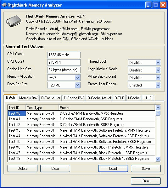
Press Add to Batch to add individual tests whatever subtest is running. RMMA tests descriptionThe RMMA test packet has 7 types of tests for estimation of key characteristics of the CPU/Chipset/RAM system. They include:
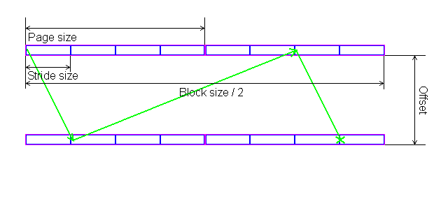
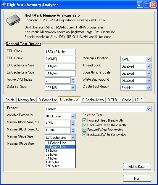
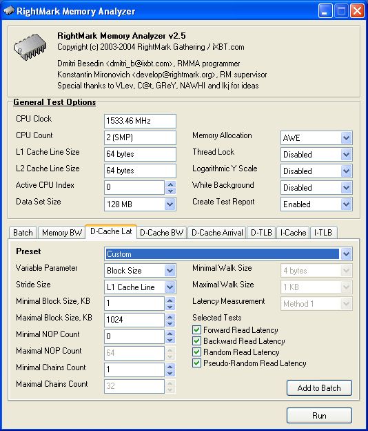
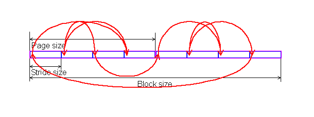
In each test you can set user settings or select one of the presets. Presets are needed for more convenient usage of test options and for comparison of systems of various classes in the same conditions. Once you select a preset the test parameters can't be changed. Benchmark #1: Memory BW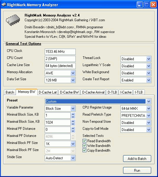 The first benchmark estimates an actual memory bandwidth of L1/L2/L3 data caches and RAM. This test measures time (in CPU clocks) of full reading/recording/copying of a data block of a certain size (which can vary or stay fixed) using some or other CPU registers (MMX, SSE, or SSE2). In case of reading and writing the test also allows for various optimizations - Software Prefetch or Block Prefetch - in order to reach the Maximal Real Read Bandwidth. The scores are calculated in bytes transferred to the CPU (from CPU) at one clock, as well as in MB/s. Below you can see settings of the first benchmark. Variable ParameterSelection of one of three test modes: Block Size - dependence of an actual memory bandwidth on data block size; Minimal Block SizeMinimal Block Size, KB, in case of Variable Parameter = Block Size; block size in other cases. Maximal Block SizeMaximal Block Size, KB, in case of Variable Parameter = Block Size. Minimal PF DistanceMinimal Software Prefetch Distance, in bytes, in case of Variable Parameter = PF Distance; Software Prefetch Distance in other cases. 0 means that the Software Prefetch mode is disabled. Maximal PF DistanceMaximal PF Distance (for Software Prefetch) in case of Variable Parameter = PF Distance. Minimal Block PF SizeMinimal Block PF Size, KB, in case of Variable Parameter = Block PF Size; Block Prefetch size in other cases. This parameter makes sense only for the Block Prefetch methods (1, 2) described below. Maximal Block PFMaximal Block PF Size, KB, in case of Variable Parameter = Block PF Size. Stride SizeStride Size in operations of reading data into cache in Block Prefetch methods (1, 2), in bytes. For more reliable results this parameter must correspond to the cache line size. That is why in this and other subtests this parameter is set to auto-detect which means that the cache line size will be automatically detected by the program at launch. CPU Register UsageCPU Register Usage - selection of registers for fulfilling read/write operations (64-bit MMX, 128-bit SSE and 128-bit SSE2). Read Prefetch TypeRead Prefetch Type defines a type of instructions used for Software Prefetch (PREFETCHNTA/T0/T1/T2); also, it enables one of Block Prefetch modes needed for taking measurements at Variable Parameter = Block PF Size. Block Prefetch 1 uses line readsets from memory to block prefetch of a certain size using MOV instructions and is recommended for AMD K7 family (Athlon/Athlon XP/MP). At the same time, in the Block Prefetch 2 method data are read with one of the Software Prefetch instructions (PREFETCHNTA). This method is recommended by AMD for K8 family (Opteron/Athlon 64/FX). Non-Temporal StoreNon-Temporal Store - direct memory access (write combining protocol) at writing. This access method writes data into memory without prereading of old data into the CPU cache levels system (without using the write allocate mode). It saves the CPU cache from unneeded data, in particular, in case of copy operations. Copy-to-Self ModeData block is copied to the same memory region where the copy block is located, i.e. the memory content doesn't actually change. This option is not enabled by default, and data copied are shifted by the offset equal to the transferred data block size. Since in this mode write operations completely get into the cache, this benchmark tests memory's ability to read data after writing (read around write). In this case the cache memory is utilized to a greater degree and the benchmark turns out to be much lighter for the memory subsystem. Note that the Non-Temporal Store and Copy-to-Self modes are incompatible. Selected TestsSelected Tests define the memory access ways. Read Bandwidth - real memory bandwidth at reading; Benchmark #2: Latency/Associativity of L1/L2 Data Cache (D-Cache Lat)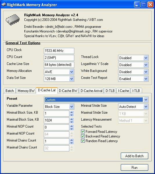 The second benchmark estimates the average/minimal latency of L1/L2 data cache and memory, L2 cache line size and L1/L2 data cache associativity. Below are its parameters and modes of its operation. Variable ParameterThere are 4 types of this test: Block Size defines dependence of cache/memory latency on a block size. This test mode demonstrates latency of various memory regions - L1, L2, L3 (if it exists) caches or RAM. A dependent access chain is created in the allocated memory, with each element containing an address of the following one. At every full read iteration stage every chain element will be addressed only once. The number of the chain elements is equal to the block size divided by the Stride Size (see below). If the stride size corresponds to the cache line length, the block size is a real characteristic of the number of data read (because data are read from RAM to L2 or from L2 to L1 line by line). The block sizes less or equal to the L1 cache allow estimating the load-use latency when accessing the L1 cache; the block size within the range (L1..L1+L2) or (L1..L2) estimates the L2 cache latency depending on the cache architecture (exclusive or inclusive), and finally (since an L3 cache is rarely used), the block size greater than L1+L2 estimates latency when accessing RAM. The chain elements execution order depends on the test method (see below). Forward Read Latency method starts from the first element and goes through all to the last one which contains the first element's addresses which allows repeating the operation multiple times. In case of Backward Read Latency the first element contains the last one's address, and reading goes from the last element to the first one. Finally, Random Read Latency test selects elements on a random basis, but the condition of selecting one element once does not change. Below you can see the principle of forward reading of the chain comprised by 8 elements. 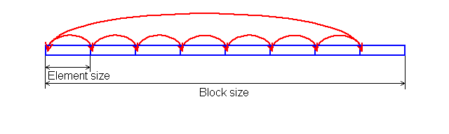 Stride Size - dependence of cache latency on stride size. This test mode makes sense only for block sizes that can get into the L2 cache and allows estimating its line length. This method of estimating of a cache line size is not the only one, the RMMA contains three such methods, the others will be studied below. Chains Count - dependence of cache latency on the number of sequential dependent access chains. It estimates L1/L2 data caches associativity. The number of chains is actually a conditional concept because in reality there is only one dependent access chain which is executed several times. The only difference between the multi-chain version and the single-chain one is that in the first case data are read from difference memory regions (their number is equal to the number of "chains"), and the offset between them is a multiple of the cache segment size. Have a look at the forward reading of an array that contains 4 chains. 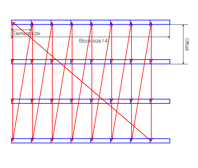 To estimate such important processor cache parameter as an associative level you should gradually increase the number of dependent access chains while maintaining the block size minimal. This fact proves that it's simple to "do harm" to the CPU cache, and it's not needed to pack it up with data. Actually, to make a "breach" in the n-way set associative cache, you just have to read n cache lines at the addresses having the offset being a multiple of the cache segment size. This is what makes this test. For example, to show inconsistency of the Pentium 4 L2 cache of 512K, with the associative level of n = 8 and a 64 bytes line one has to read only 8 x 64 = 512 bytes, i.e. it's needed to take less than 0.1% of its size(!). The minimal cache segment size in the current test version is equal to 1MB. Such a large value guarantees that the test will correct define the L2/L3 cache associative level even in systems having a large cache (note that the cache segment equal to 1MB corresponds to a 8MB L3 data cache with the associative level of 8). NOP Count - dependence of latency of the memory region selected (L2 cache or memory) on the number of voids between two successive accesses to the region selected (L2 cache or memory). These operations called NOP are not related to the cache access but they bring a fixed time gap between two successive accesses to different cache/memory lines. It unloads the data bus between L1-L2 or L2-RAM to make the latency in accessing a selected memory area as low as possible. In the current RMMA version such NOPs are based on x86 ALU or eax, edx (eax stores the chain element address, and edx is initialized with 0); this command suits well for testing a good deal of modern processors. Minimal Block Size, KBMinimal Block Size, KB, in case of Variable Parameter = Block Size; Block size in other cases. Maximal Block Size, KBMaximal Block Size, KB, in case of Variable Parameter = Block Size. Minimal NOP CountMinimal NOP Count in case of Variable Parameter = NOP Count; NOP count in other cases. Maximal NOP CountMaximal NOP Count in case of Variable Parameter = NOP Count. Minimal Chains CountMinimal Chains Count - a minimal number of successive dependent access chains in case of Variable Parameter = Chains Count; the number of successive dependent access chains in other cases. The offset of every such dependent access chain from its neighbors is equal to the value which is a multiple of the maximum possible cache segment size. Maximal Chains CountMaximal Chains Count - a maximal number of successive dependent access chains in case of Variable Parameter = Chains Count. Minimal Stride SizeMinimal Stride Size, bytes, in the dependent access chain (in each chain if they are more than one) in case of Variable Parameter = Stride Size; stride size in a dependent access chain in other cases. Maximal Stride SizeMaximal Stride Size in a dependent access chain in case of Variable Parameter = Stride Size. Latency MeasurementLatency Measurement technique (the parameters can be configured only if Variable Parameter = NOP Count). In Method 1 an ordinary dependent access chain with a varying number of NOPs (see above (edx = 0)) is used to determine the minimal latency : // loading of next chain elementNevertheless, in some cases (if the speculative loading works effectively) the minimal cache latency may not be achieved. For such cases there's an alternative RMMA method (Method 2) which uses a different chain read code (ebx = edx = 0): // bus unloading, fixed number of NOPs Selected TestsSelected Tests define the memory access ways when testing latency. Forward Read Latency - forward sequential access latency; Benchmark #3: Real L1/L2 Data Cache Bus Bandwidth (D-Cache BW)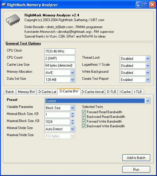 This benchmark estimates a real L1-L2 cache bus bandwidth (or L2-RAM bus bandwidth). It's the simplest test in RMMA regarding its configuring. It's based on the method used in the real L1/L2/RAM bus bandwidth test (Benchmark #1). But in this case memory read/write operations are carried out line by line, i.e. with the stride equal to the cache line length and with CPU' ALU registers. Both forward and backward access modes are supported. Test parameters: Variable ParameterVariable Parameter defines one of two test modes: Block Size - dependence of a real data bus bandwidth on the data block size; Minimal Block Size, KBMinimal Block Size, KB, in case of Variable Parameter = Block Size; Block Size in other cases. A value less than 1.5 times L1 cache will yield senseless results. This test doesn't estimate a bandwidth of the L1-LSU-registers tandem because loading of data from L1 into LSU (Load-Store Unit) and then to CPU registers is not fulfilled line by line. To estimate the L1-LSU bandwidth it's better to run the first test (Memory BW) within the range of block sizes which can get into the L1 cache. Maximal Block Size, KBA value lower than the L2 cache size (inclusive cache architecture) or L1+L2 (exclusive cache architecture) allows estimating a real L1-L2 bus bandwidth. In case of the Block Size values ranging from L1+L2 to some greater value this benchmark estimates the maximal real memory bandwidth at reading/writing of full cache lines, which in some cases turns out to be greater than the maximal real bandwidth in case of total data reading/writing. Minimal Stride SizeMinimal Stride Size in cache accessing at reading/writing in case of Variable Parameter = Stride Size; Cache access Stride Size in other cases. Selected TestsSelected Tests define a type of measurements. Forward Read Bandwidth - forward sequential cache line reading; Benchmark #4: L1/L2 (D-Cache) Arrival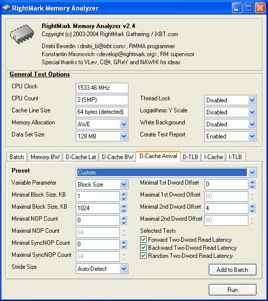 The fourth benchmark estimates L1-L2 bus realization features (bit capacity, multiplexing) for some processors with an exclusive cache architecture, in particular, for AMD K7/K8 processors. This test actually measures the total latency of two accesses to the same cache line which are separated by a certain value. The measurement method is identical to the one in Method #2 except the fact that two consecutive chain elements are located in the same cache line. 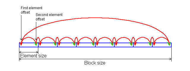 Besides, the fourth test can be used to calculate the L2 cache line size (this is the third way in RMMA to estimate it, and it's used for its estimation at the program startup). The fourth test parameters are as follows: Variable ParameterVariable Parameter define one of five test types: Block Size - dependence of the total latency on the block size. Minimal Block Size, KBMinimal Block Size, KB, in case of Variable Parameter = Block Size; total Block Size in other cases. Maximal Block Size, KBMaximal Block Size, KB, in case of Variable Parameter = Block Size. Minimal NOP CountMinimal NOP Count defines the minimal number of NOPs between two successive accesses to adjacent cache lines in case of Variable Parameter = NOP Count; the number of NOPs between two successive accesses to adjacent cache lines in other cases. Maximal NOP CountMaximal NOP Count defines the maximal number of NOPs between two successive accesses to adjacent cache lines in case of Variable Parameter = NOP Count. Minimal SyncNOP CountMinimal SyncNOP Count defines the minimal number of NOPs between two successive accesses to the same cache line in case of Variable Parameter = SyncNOP Count; the number of NOPs between two successive accesses to the same cache line in other cases. Maximal SyncNOP CountMaximal SyncNOP Count defines the maximal number of NOPs between two successive accesses to the same cache line in case of Variable Parameter = SyncNOP Count. Stride SizeMinimal Stride Size, in bytes, in the dependent access chain between two successive accesses to consecutive cache lines. Minimal 1st Dword OffsetMinimal 1st Dword Offset within the cache line, in bytes, in case of Variable Parameter = 1st DW Offset; 1st Dword Offset within the cache line in other cases. Maximal 1st Dword OffsetMaximal 1st Dword Offset within the cache line in case of Variable Parameter = 1st DW Offset. Minimal 2nd Dword OffsetMinimal 2nd Dword Offset within the cache line, in bytes, in case of Variable Parameter = 2st DW Offset; 2st Dword Offset within the cache line in other cases. The 2nd DW Offset is calculated relative to the 1st Dword offset modulo stride size (cache line size): 2nd_Dword_Offset = (2nd_Dword_Offset + 1st_Dword_Offset) % Stride_Size Maximal 2nd Dword OffsetMaximal 2nd Dword Offset within the cache line in case of Variable Parameter = 2nd DW Offset. Selected TestsSelected Tests define a way of testing the latency of the double access. Forward Two-Dword Read Latency; Benchmark #5: Data Translation Lookaside Buffer Test (D-TLB)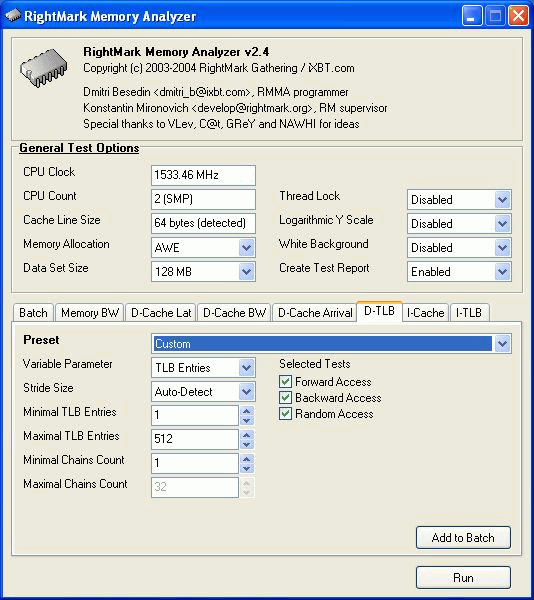 The fifth test defines the size and associative level of the Translation Lookaside Buffer (L1/L2 D-TLB). Actually, it measures latency when accessing the L1 cache provided that every next cache line is loaded from the next memory page (not the same). 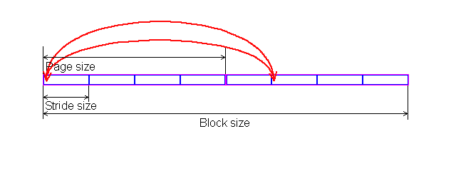 (The memory page size in real operating systems is much greater (e.g. 4096 bytes), than in our scheme which houses only 4 cache lines).So, if the number of pages used is less than the TLB size the test calculates L1 cache's own latency (TLB hit). Otherwise, it measures the L1 cache latency in case of TLB miss. Note that the Maximal TLB Entries mustn't be greater than the number of L1 cache lines, otherwise the graph will have a jump related with the transition from L1 to L2, but not with the D-TLB structure size. But the overall size of TLB levels is always less than the number of cache lines which can be put into the L1 cache. Test settings: Variable ParameterVariable Parameter defines one of two test modes. TLB Entries - dependence of latency when accessing the L1 cache on the number of memory pages used. 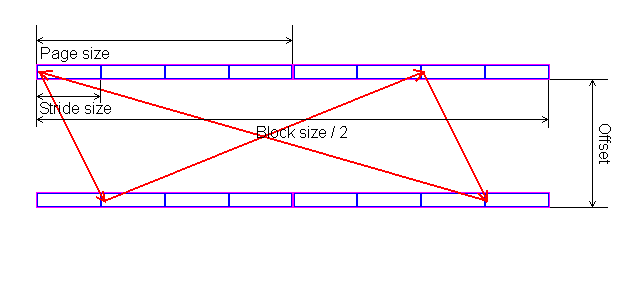 Stride SizeStride Size in the dependent access chain, in bytes. Minimal TLB EntriesMinimal TLB Entries used for reading cache lines in case of Variable Parameter = TLB Entries; TLB Entries in other cases. Maximal TLB EntriesMaximal TLB Entries in case of Variable Parameter = TLB Entries. Minimal Chains CountMinimal Chains Count defines the minimal number of sequential dependent access chains in case of Variable Parameter = Chains Count; the number of sequential dependent access chains in other cases. Maximal Chains CountMaximal Chains Count defines the maximal number of sequential dependent access chains in case of Variable Parameter = Chains Count. Selected TestsSelected Tests define the ways of testing. Forward Access; Benchmark #6: Instruction Cache Test (I-Cache) The sixth test estimates effectiveness of decoding/execution of certain simple CPU instructions (ALU/FPU/MMX), and efficiency of operation of the L1 instructions cache and its associative level. This test is of special interest for estimating the effective Trace Cache size of Pentium 4 processors in case of decoding/execution of various instructions. Test parameters. Variable ParameterDefines one of three types of this benchmark: Block Size - dependence of decode bandwidth on the code block size (Decode Bandwidth is the speed of sequence of operations of reading, decoding and execution of instructions by the CPU). The test method includes on-the-fly creation of a code block of a certain size on the fly (in runtime) and measurement of CPU clocks taken for its execution. The last instruction in the code block in all cases is the return instruction (RET). 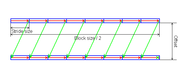 Prefixes Count - dependence of decode bandwidth for [pref]nNOP instructions on the number of prefixes used (pref = 0x66, operand-size override prefix). Minimal Block Size, KBMinimal Code Block Size, KB, in case of Variable Parameter = Block Size; Code Block Size in other cases. Maximal Block Size, KBMaximal Code Block Size, KB, in case of Variable Parameter = Block Size. Minimal Chains CountMinimal Chains Count defines the minimal number of sequential access chains in case of Variable Parameter = Chains Count; the number of sequential access chains in other cases. Maximal Chains CountMaximal Chains Count defines the maximal number of sequential access chains in case of Variable Parameter = Chains Count. Minimal Prefixes Count, Maximal Prefixes CountMinimal Prefixes Count, Maximal Prefixes Count in case of Variable Parameter = Prefixes Count. Unavailable in other cases. Stride SizeStride Size is the minimal size of the code executed in this chain which includes transition to the neighboring chain. It's recommended that the stride size is equal to the instructions cache line size. Instructions TypeInstructions Type is a type of decoded/executable instructions: ALU - arithmetic and logic integer operations using general-purpose registers; Instructions SubtypeInstructions Subtype is a subtype of decoded/executable instructions. It
depends on an instruction type selected. An instruction size in bytes is
given in parentheses.
Benchmark #7: Instruction Translation Lookaside Buffer Test (I-TLB)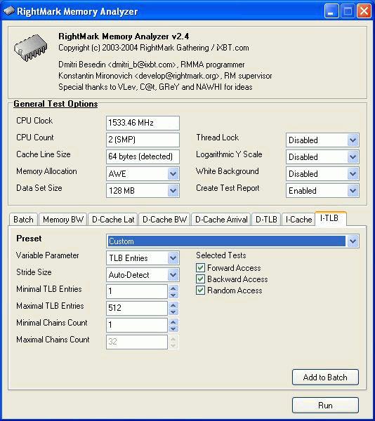 The last RMMA benchmark measures size and associative level of the Instructions Translation Lookaside Buffer (L1/L2 I-TLB). The test settings are identical to the Benchmark #5: Variable ParameterVariable Parameter defines one of two types of the test modes: TLB Entries - dependence of latency when accessing the L1i cache on the number of memory pages used. Minimal TLB EntriesMinimal TLB Entries used for reading L1i cache lines in case of Variable Parameter = TLB Entries; TLB Entries in other cases. Maximal TLB EntriesMaximal TLB Entries in case of Variable Parameter = TLB Entries. Minimal Chains CountMinimal Chains Count defines the minimal number of sequential dependent access chains in case of Variable Parameter = Chains Count; the number of sequential dependent access chains in other cases. Maximal Chains CountMaximal Chains Count defines the maximal number of sequential dependent access chains in case of Variable Parameter = Chains Count. Selected TestsSelected Tests define the ways of testing.
Forward Access;The latency estimated in this test actually defineS latency in execution of an instructions tandem mov ecx, address_valueat their different number and relative positions. Nevertheless, such characteristic is acceptable for defining the I-TLB levels structure and their associativity. Appendix 1: RightMark Memory Analyzer 2.5
|
|
Article navigation: |
| blog comments powered by Disqus |
| Most Popular Reviews | More RSS |
 |
Comparing old, cheap solutions from AMD with new, budget offerings from Intel.
February 1, 2013 · Processor Roundups |
 |
Inno3D GeForce GTX 670 iChill, Inno3D GeForce GTX 660 Ti Graphics Cards A couple of mid-range adapters with original cooling systems.
January 30, 2013 · Video cards: NVIDIA GPUs |
 |
Creative Sound Blaster X-Fi Surround 5.1 An external X-Fi solution in tests.
September 9, 2008 · Sound Cards |
 |
The first worthwhile Piledriver CPU.
September 11, 2012 · Processors: AMD |
 |
Consumed Power, Energy Consumption: Ivy Bridge vs. Sandy Bridge Trying out the new method.
September 18, 2012 · Processors: Intel |
| Latest Reviews | More RSS |
 |
Retested all graphics cards with the new drivers.
Oct 18, 2013 · 3Digests
|
|
Added new benchmarks: BioShock Infinite and Metro: Last Light.
Sep 06, 2013 · 3Digests
|
|
Added the test results of NVIDIA GeForce GTX 760 and AMD Radeon HD 7730.
Aug 05, 2013 · 3Digests
|
 |
Gainward GeForce GTX 650 Ti BOOST 2GB Golden Sample Graphics Card An excellent hybrid of GeForce GTX 650 Ti and GeForce GTX 660.
Jun 24, 2013 · Video cards: NVIDIA GPUs
|
|
Added the test results of NVIDIA GeForce GTX 770/780.
Jun 03, 2013 · 3Digests
|
| Latest News | More RSS |
Platform · Video · Multimedia · Mobile · Other || About us & Privacy policy · Twitter · Facebook
Copyright © Byrds Research & Publishing, Ltd., 1997–2011. All rights reserved.