 |
||
|
||
| ||
|
||
|
||
| ||
 Mind-blowing performance.
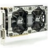
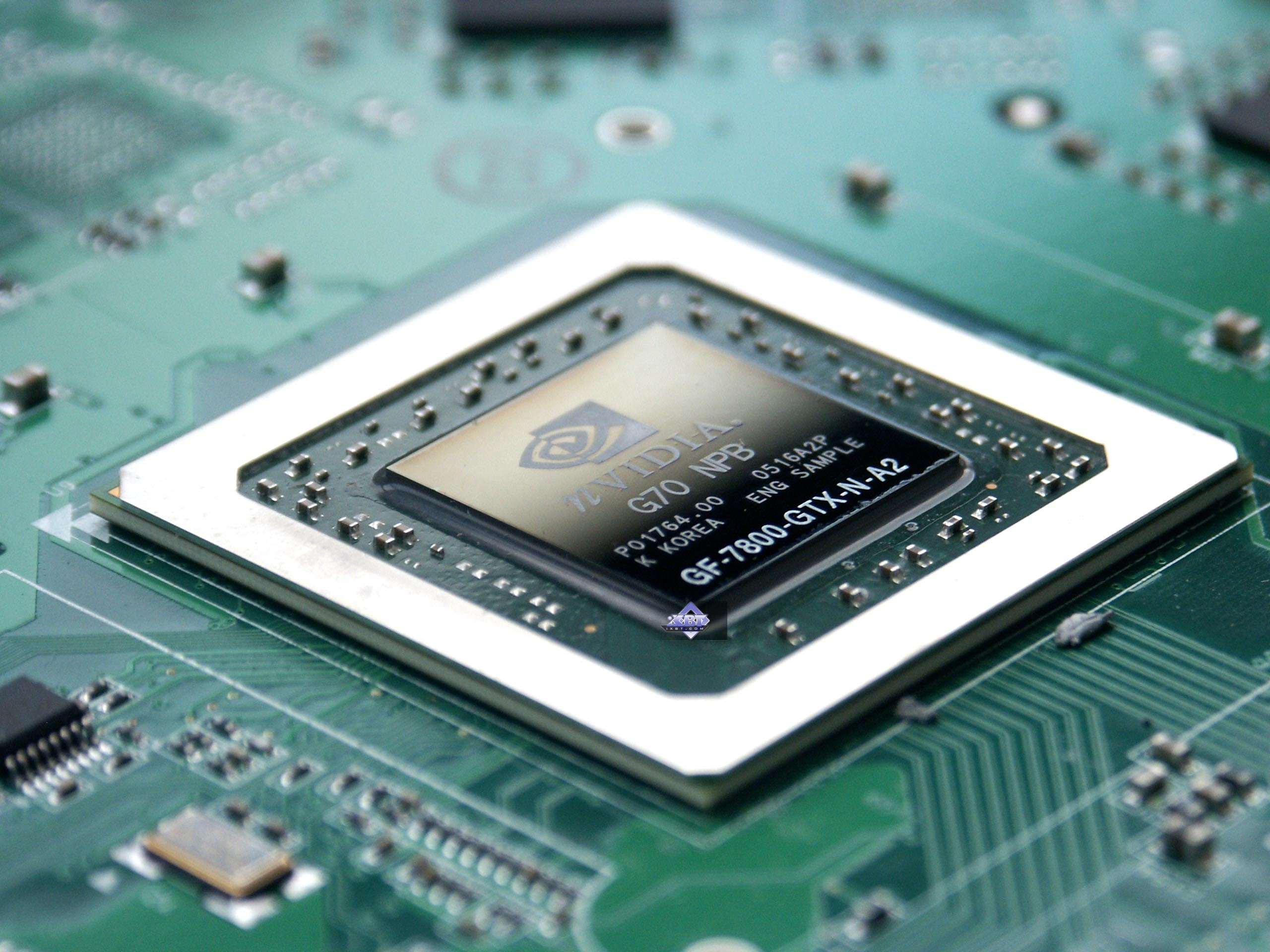
The protracted wait for new video accelerators is over. Here is it, the new top model from NVIDIA. If all goes well, in autumn we shall see it competing with the new top solution from ATI, which (it's no longer a secret) will also support Shaders 3.0. We'll see who will win! But now let's start our indepth examination of the GeForce 7800 GTX. It's become a tradition to start with specifications, diagrams, and a theoretical part. GeForce 7800 GTX (codenamed G70) SpecificationsA new codename of the chip. What does NVIDIA mean? Running a few steps forward, I want to note that despite the noticeable performance growth, this architecture is not principally new — it's an improved but well-known architecture, used in the NV4X series. Thus, the chip has got the new codename for a different reason. Perhaps NV47 would have sounded too ordinary, while its architectural differences from the NV45 are actually noticeable and more pronounced than in case of regular tuning. Or perhaps there are other reasons, we can only guess. Before you read this article, you had better look through the fundamental
materials on DX Current, DX
Next and Longhorn that describe various
aspects of modern hardware video accelerators in general and architectural
features of NVIDIA and ATI's products in particular. You may also
get some useful information on the previous flagship architecture
from NVIDIA in the following article: And now let's proceed to the specifications of the new product: Official GeForce 7800 specifications
Reference card GeForce 7800 GTX specifications
The specs are impressive, though they inherit much from the previous flagships based on NV40 and NV45. Let's note the key differences:
So, the designers obviously pursued two objectives in the process of creating the new accelerator — to reduce power consumption and to drastically increase performance. As Shader Model 3.0 was already implemented in the previous generation of NVIDIA accelerators, and the next rendering model (WGF 2.0) is not yet worked out in detail, this product looks quite logical and expectable. Good news: pixel processors are not only increased in number, they also have become more efficient. The only question is why there is no filtering for texture sampling in vertex processors — this step seems quite logical. But probably this solution would have taken too much resources and NVIDIA engineers decided to spend them on other objectives, namely on reinforcing pixel processors and increasing their number. Well, the next generation of accelerators will comply with WGF 2.0 and consequently will finally get rid of the disappointing asymmetry in texture unit capacities between vertex and pixel shaders. Another objective is the large-scale introduction of HDTV support as a new universal (in future) standard. Architecture of the acceleratorAnd now let's traditionally proceed to the general diagram of the chip: 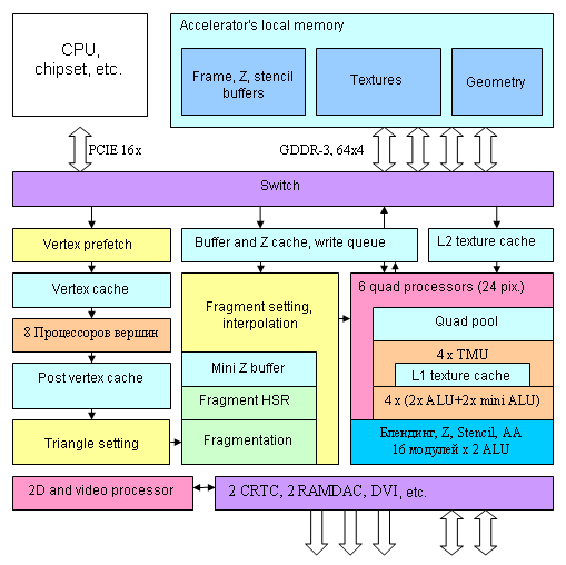
The key differences of this diagram from NV45 are 8 vertex processors and 6 quad processors (all in all, 4*6=24 pixels are processed) instead of 4 with more ALUs for each processor. Pay your attention to the AA, blending, and writing unit, located outside the quad processor on the diagram. The fact is that even though the number of pixel processors is increased by 1.5, the number of modules responsible for writing the results remains the same — 16. That is the new chip can calculate shaders much faster, simultaneously for 24 pixels, but it still writes up to 16 full pixels per cycle. It's actually quite enough — memory wouldn't cope with more pixels per cycle. Besides, modern applications spend several dozens of commands before calculating and writing a single pixel. That's why increasing the number of pixel processors and retaining the same number of modules resposible for writing looks quite a balanced and logical solution. Such solutions were previously used in low end NVIDIA chips (e.g. GeForce 6200), which had a sterling quad processor, but curtailed writing modules (in terms of the number of units and no FP16 blending). Pixel pipelineSo, here is the architecture of the pixel section: 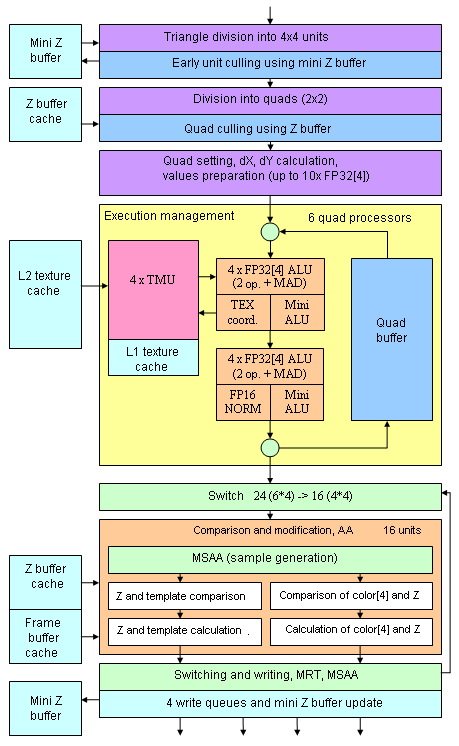
Have a look at the yellow unit of the pixel processor (quad processor). One can say that the architecture used in NV40/45 has been "turboed" — two full vector ALUs, which can execute two different operations over four components, were supplemented with two scalar mini ALUs for parallel execution of simple operations. Now ALUs can execute MAD (simultaneous multiplication and addition) without any penalty. This solution is claimed to lead to twofold performance increase of some heavy and convenient shaders (which manage to load regular ALUs and mini-ALUs) and to the 1.5-fold growth of shader performance on average. Indeed, MAD is a very popular operation that can be often found in typical pixel shaders. NVIDIA specialists came up with this ALU configuration after the statistical research of many various game shaders. But the figure mentioned (1.5-fold) looks too optimistic, which is only typical of NVIDIA PR department. Later on we shall see what influence this architectural element will have on our synthetic and game tests. Adding small simplified and special ALUs is an old NVIDIA's trick, the company resorted to it several times to ensure noticeable performance gain in pixel units by only slightly increasing the number of transistors. For example, even the NV4X had a special unit for normalizing FP16[4] vectors (it is connected to the second main ALU and entitled FP16 NORM on the diagram). The G70 continues the tradition - such a unit allows considerable performance gain in pixel shaders due to "free" normalization of vectors each time a quad passes though a pipeline of the processor. Interestingly, the normalization operation is coded in shaders as a sequence of several commands, the driver must detect it and substitute it with a single call to this special unit. But in practice this detect process is rather efficient, especially if a shader was compiled from HLSL. Thus, NVIDIA's pixel processors don't spend several cycles on vector normalization as ATI does (it's important not to forget about the format limitation - FP16, that is half-precision). What concerns texture units, everything remains the same — one unit per pixel (that is four units in a quad processor), native L1 Cache in each quad processor, texture filtering in integer or FP16 component format, up to 4 components inclusive (FP16[4]). Texture sampling in FP32 component format is possible only without hardware filtering — you will either have to do without it or program it in a pixel shader, having spent a dozen of instructions or more. However, the same situation happened before - sterling support for FP32 components will probably be introduced only in the next generation of architectures. The array of 6 quad processors is followed by the switch that distributes calculated quads among 16 units of Z generation, AA, and blending (to be more exact, among 4 groups of 4 units processing the entire quad, because geometric consistency must not be lost, as it will be required for writing and compressing colors and Z buffer). Each unit can generate, check up, and write two Z-values or one Z-value and one color value per cycle. Double-sided stencil buffer operations. Besides, one such unit executes 2x multisampling "free-of-charge", 4x mode requires two passes through this unit, that is two cycles. But there are exceptions. Let's sum up features of such units:
There appear so many conditions due to many hardware ALUs, necessary for MSAA operations, generating Z-values, comparing and blending color. NVIDIA tries to optimize transistor usage and employs the same ALUs for different purposes depending on a task. That's why the floating point format excludes MSAA and FP32 excludes blending. The high consumption of transistors is one of the reasons to retain 16 units instead of 24 according to the number of pixel processors. This solution implies that most transistors in these units may (and shall) be idle in modern applications with long shaders, even in 4xAA mode; and memory, which bandwidth is practically not increased compared to GeForce 6800 Ultra, will not allow to write even 16 full pixels per cycle into a frame buffer. As these units are asynchronous to pixel processors (they are calculating Z-values and blending, when shaders calculate colors for the next pixels), 16 units are a justified, even obvious solution. But some restrictions due to FP formats are disappointing but typical of our transition period on the way to symmetric architectures, which will allow all operations with all available data formats without any performance losses, as allowed by flexible modern CPUs in most cases. Vertex pipelineNo special changes here: 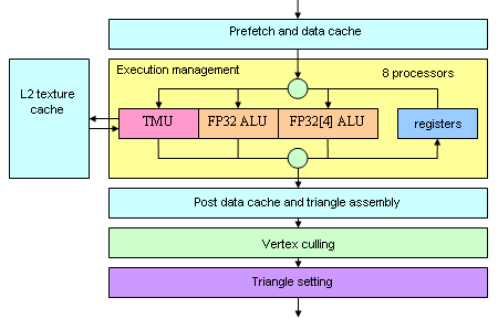
Everything is familiar by the NV4x family, only the number of vertex processors is increased from 6 to 8. Texture sampling in vertex processors is still nominal — both in performance and in features. Filtering is not available for any format — only dot sampling, but its performance (according to our tests) is not high compared to pixel processors. However, this SM 3.0 feature is rarely used in real applications so far, so we can resign ourselves to this "Cinderella" status. But in the heart of hearts we'd like to see the future WGF 2.0 as soon as possible, at least in terms of symmetric features with textures in vertex and pixel processors. Running a few steps forward, I want to note that some aspects of operations with geometry (caching vertices) were actually improved. We are going to examine this issue in the second part of the article. Data formats that the accelerator processesA short reference. There are the following data representation (storage) formats (per component, from 1 to 4):
The data is processed (calculations) in the following formats:
A new great AA featureAnd now let's talk about the new important features of the accelerator, which are not displayed on the above diagrams. This accelerator features the gamma-correct MSAA (which has been used in ATI chips since the R3XX) and Transparent Supersampling — AA innovation implemented in this chip. As is well known, the main problem of MSAA is that it smoothes only polygon edges. If a polygon is transparent or semitransparent (for example, glass or a wired fence in a game, where transparent pixels interlace with non-transparent ones), the polygon edges are not smoothed with the background image resulting in sharp edges. But then we don't have to calculate colors for each sample, we can do with just separate Z-values and the color is the same for all samples. The main problem (steps at polygon edges) is efficiently resolved by this method. But it does not cope with transparent polygons. The second method — SSAA (supersampling) honestly calculates all color values for all samples and we get the correct picture even through semi-transparent polygons with sharp borders between transparent and non-transparent areas. But in this case we noticeably lose performance — we have to execute much more pixel shaders — by as many as we have samples, 2 or 4 times as many. What can be done about it? We are offered the following way out: Sterling SSAA snaps into action automatically for transparent polygons (there is also an option: special emulation of MSAA that takes transparency into account), the other polygons are processed with vanilla MSAA.
A simple but quite an effective solution. Hardware changes are not so great — we store sample depth and color in both cases anyway. All we need is to automatically switch the AA sampling mode depending on the transparency in blending settings of triangles (this choice is hardly made on a more precise level than a whole triangle; it must be obviously done automatically). In the next part we shall analyze its effect on video performance and quality in practice and shall provide more details on this innovation.
 And now let's proceed to the first practical aspects - video card's description and synthetic tests. NVIDIA GeForce 7800 GTX 256MB PCI-E: Part 2: Video card's description, testbed configuration, synthetic test resultsWrite a comment below. No registration needed!
|
Platform · Video · Multimedia · Mobile · Other || About us & Privacy policy · Twitter · Facebook Copyright © Byrds Research & Publishing, Ltd., 1997–2011. All rights reserved. |